Semiconductor chip and semiconductor chip package comprising semiconductor chip

a semiconductor chip and semiconductor chip technology, which is applied in the direction of digital storage, instruments, agricultural tools and machines, etc., can solve the problems of insufficient number of test channels for a psram device disposed in the dual chip package, the restriction of the number of channels available for testing the device, etc., and achieve the effect of improving the testing environment of the semiconductor chip

Inactive Publication Date: 2008-09-02
SAMSUNG ELECTRONICS CO LTD
View PDF11 Cites 18 Cited by
  • Summary
  • Abstract
  • Description
  • Claims
  • Application Information

AI Technical Summary

Benefits of technology

[0009]Embodiments of the invention provide a semiconductor chip and a semiconductor package comprising the semiconductor chip in which fewer option pads of the semiconductor chip are used for the dual chip mode in order to improve the testing environment of the semiconductor chip.

Problems solved by technology

Because of the high degree of integration and the large storage capacity of the dual chip package, the number of channels available for use in testing the device is restricted.
Specifically, the number of test channels for a PSRAM device disposed in the dual chip package is insufficient (compared with a DRAM device disposed in the dual chip package) because a low address signal and a column address signal are supplied through separate pads of a PSRAM device.

Method used


Image

  • Semiconductor chip and semiconductor chip package comprising semiconductor chip
  • Semiconductor chip and semiconductor chip package comprising semiconductor chip
  • Semiconductor chip and semiconductor chip package comprising semiconductor chip

Examples


Embodiment Construction

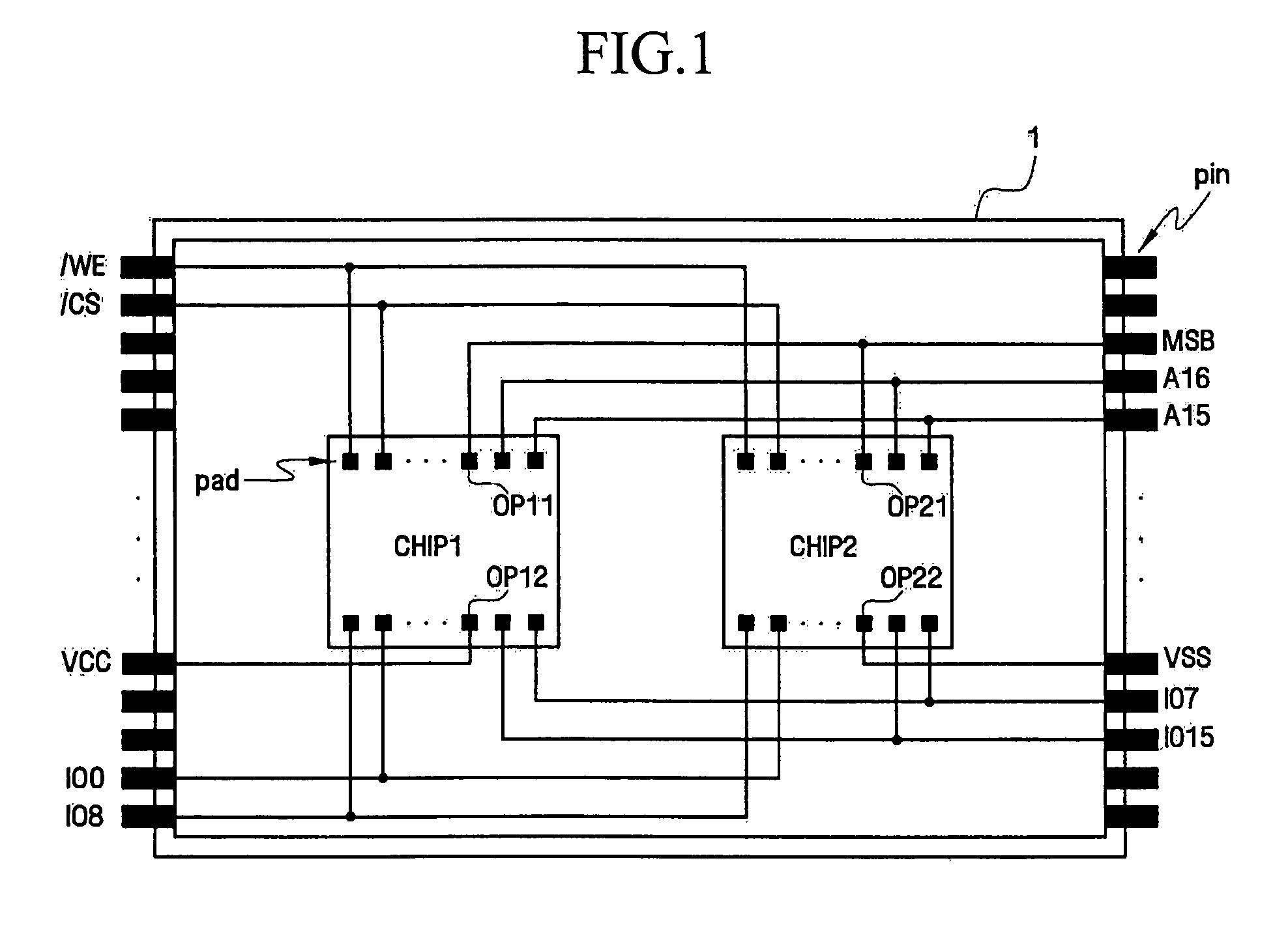
[0020]FIG. 1 is a layout diagram illustrating a semiconductor chip in accordance with an embodiment of the invention.

[0021]Referring to FIG. 1, a semiconductor chip package 1, in accordance with an embodiment of the invention, is a dual chip package and comprises a first semiconductor chip CHIP1 and a second semiconductor chip CHIP2.

[0022]First and second semiconductor chips CHIP1 and CHIP2 may be substantially the same. Specifically, first and second semiconductor chips CHIP1 and CHIP2 may have the same pad layout, storage capacity, and address coding scheme. Therefore, first and second semiconductor chips CHIP1 and CHIP2 may be created from the same wafer.

[0023]Further, package pins of semiconductor chip package 1 such as an address pin, a control pin, and a data pin may be connected to both first semiconductor chip CHIP1 and second semiconductor chip CHIP2. Therefore, when seen from outside of semiconductor chip package 1, first and second semiconductor chips CHIP1 and CHIP2 appe...


PUM


Abstract

Embodiments of the invention provide a semiconductor chip and a semiconductor chip package comprising a semiconductor chip. In one embodiment, the invention provides a semiconductor chip comprising a memory cell array, a control circuit, and a chip selection signal generating circuit electrically connected to first and second option pads. In the semiconductor chip, the chip selection signal generating circuit is enabled in accordance with a dual chip enable signal, and the control circuit is enabled and disabled in accordance with the chip selection signal received from the chip selection signal generating circuit. In addition, the chip selection signal generating circuit is adapted to generate a chip selection signal in accordance with signals received through the first and second option pads, respectively.

Description

BACKGROUND[0001]1. Field of the Invention[0002]Embodiments of the invention relate to a semiconductor chip and a semiconductor chip package comprising a semiconductor chip. In particular, embodiments of the invention relate to a semiconductor chip that requires the use of fewer option pads to operate in a dual chip mode, and a semiconductor chip package comprising the semiconductor chip.[0003]This application claims priority to Korean Patent Application No. 10-2006-0013123, filed on Feb. 10, 2006, the subject matter of which is hereby incorporated by reference in its entirety.[0004]2. Description of Related Art[0005]In order to achieve a relatively high degree of integration and relatively large storage capacity in a semiconductor device, a technique for mounting a plurality of individual semiconductor chips in one package has been developed. Such a technique, in which two identical semiconductor chips are mounted in one package, is disclosed, for example, in U.S. Pat. No. 6,366,487...

Claims


Application Information

Patent Timeline
Patent Type & Authority Patents(United States)
IPC IPC(8): G11C5/06
CPCG11C5/04G11C5/066G11C8/06G11C29/48G11C11/40615G11C29/1201G11C8/12A01F12/22A01F7/02A01F11/00
Inventor SEO, EUN-SUNGKIM, MI-JOKIM, SOO-YOUNG
Owner SAMSUNG ELECTRONICS CO LTD
Why Eureka
Try Eureka