Multiple sampling sample and hold architectures

a technology which is applied in the field of multi-sample and hold architecture, can solve the problems of more power consumption of amplifiers, more idle times of one half of a clock signal cycle in each of tracking and hold modes, and shorter available settling time, so as to achieve a given distortion level and shorten the available settling time , the effect of increasing the current capacity

Active Publication Date: 2008-09-09
ANALOG DEVICES INC
View PDF6 Cites 10 Cited by
  • Summary
  • Abstract
  • Description
  • Claims
  • Application Information

AI Technical Summary

Benefits of technology

[0002]The sample and hold circuit is placed ahead of the circuit element or elements that do the actual conversion to digital values. Because the conversion takes a finite amount of time, it is necessary to provide the converter circuit with a stable, fixed, signal for the duration of the sampling time. The sample and hold circuit is the element that performs this operation. The sample and hold circuit consists of some sort of element that can sample the input signal for a short period of time, corresponding to the conversion time, and then provide this sampled value to the actual converter circuitry. The sample and hold may simply take a brief sample of the input signal or it may average the input signal over the sampling interval.
[0006]A shorter available settling time requires a higher power consumption to achieve a given distortion level. This is because the time it takes a capacitor to charge to the buffer voltage is dependent on the current capacity of the buffer amplifier. Similarly, the time it takes the output amplifier to charge up to the voltage held on the capacitor is dependent on the current capacity of the output amplifier. The higher the current capacity, the more power the amplifiers consume. In order to achieve high accuracy in the tracking of the output of the amplifier to the input, shorter settling times are desirable. Therefore, the idle times of one half of a clock signal cycle in each of the tracking and hold modes require higher power consumption.
[0007]It would therefore be desirable to provide an alternative sample and hold architecture that utilized idle times and lowered the requirement for power consumption in the buffer and output amplifiers.

Problems solved by technology

A shorter available settling time requires a higher power consumption to achieve a given distortion level.
The higher the current capacity, the more power the amplifiers consume.
Therefore, the idle times of one half of a clock signal cycle in each of the tracking and hold modes require higher power consumption.

Method used


Image

  • Multiple sampling sample and hold architectures
  • Multiple sampling sample and hold architectures
  • Multiple sampling sample and hold architectures

Examples


Embodiment Construction

[0026]For a general understanding, reference is made to the drawings. In the drawings, like references have been used throughout to designate identical or equivalent elements. It is also noted that the drawings may not have been drawn to scale and that certain regions may have been purposely drawn disproportionately so that the features and concepts could be properly illustrated.

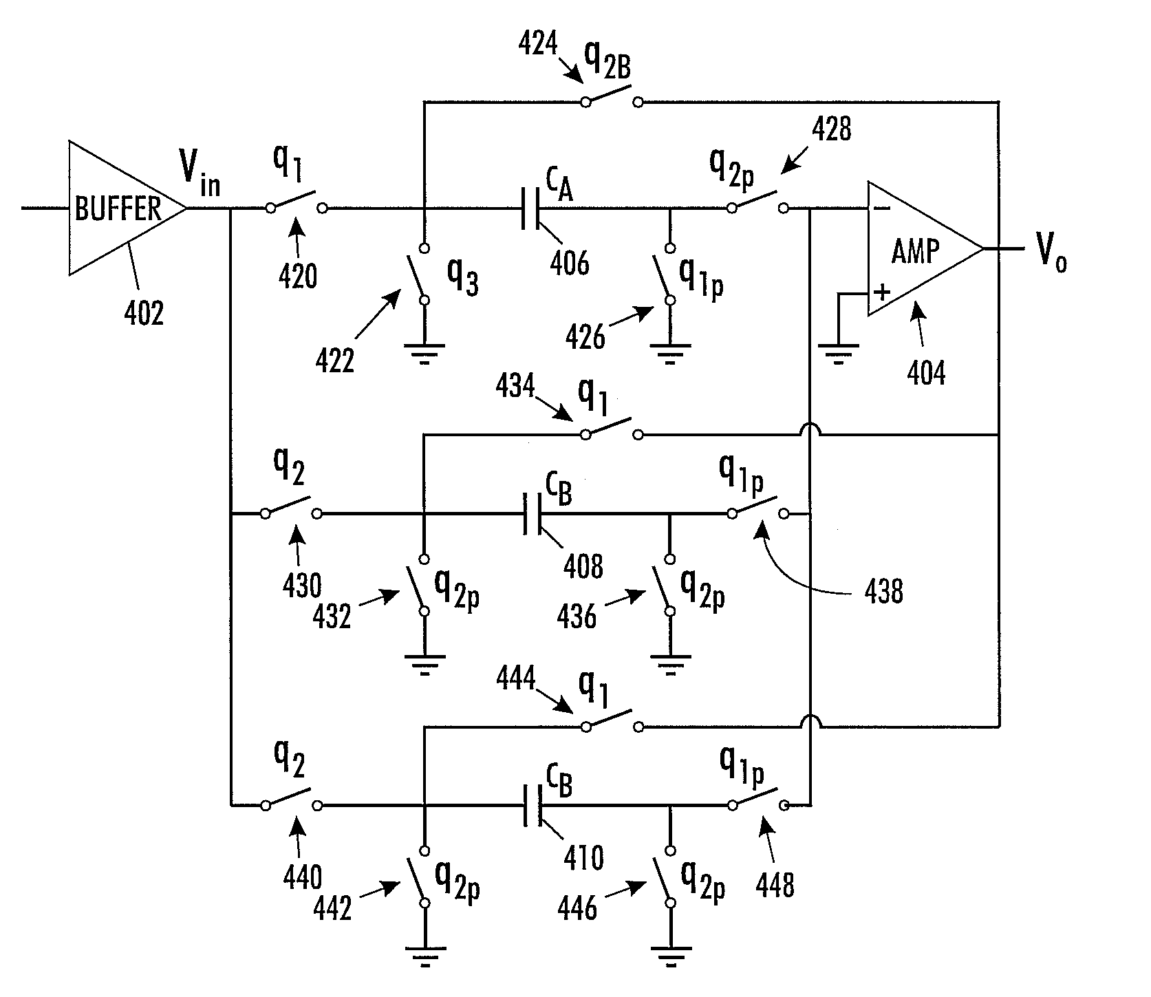
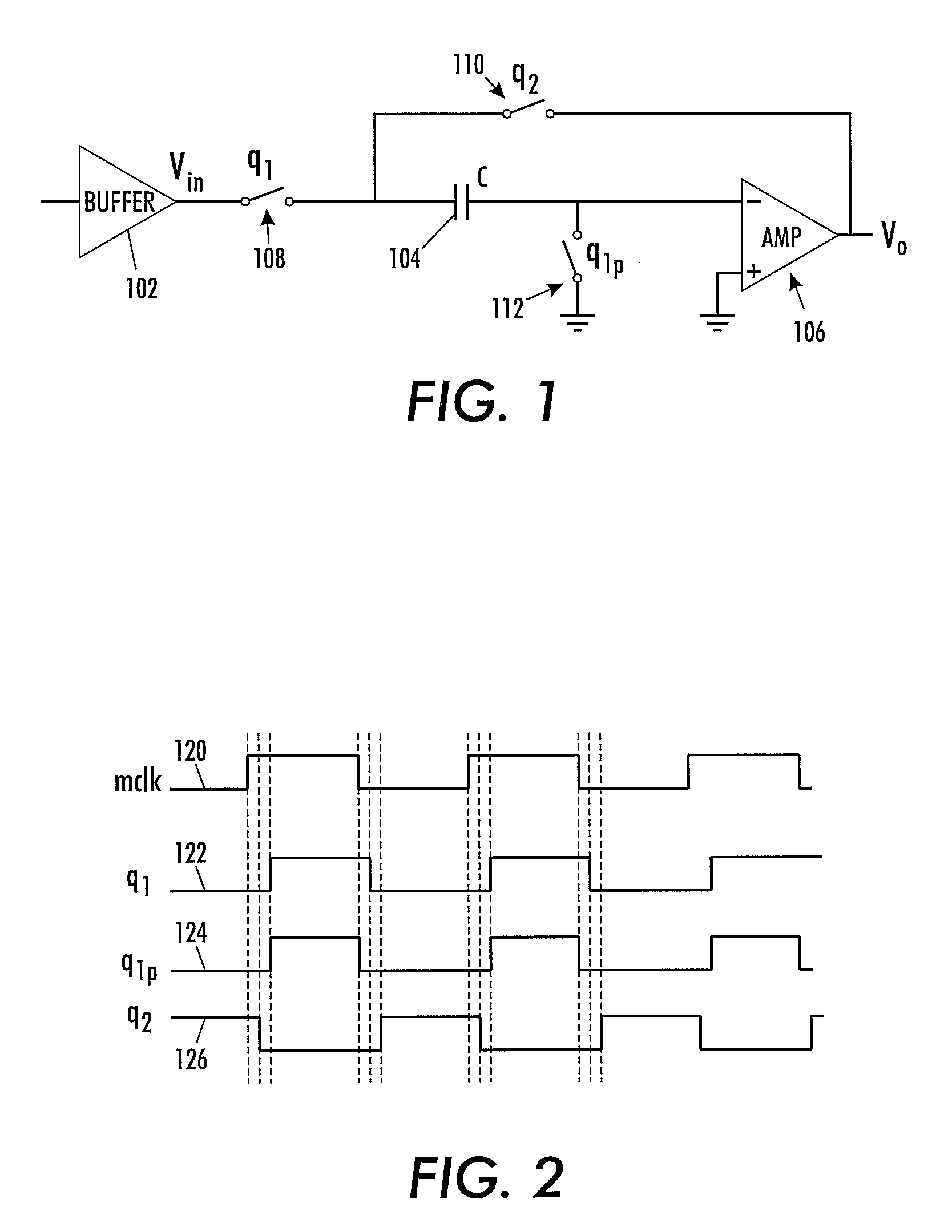
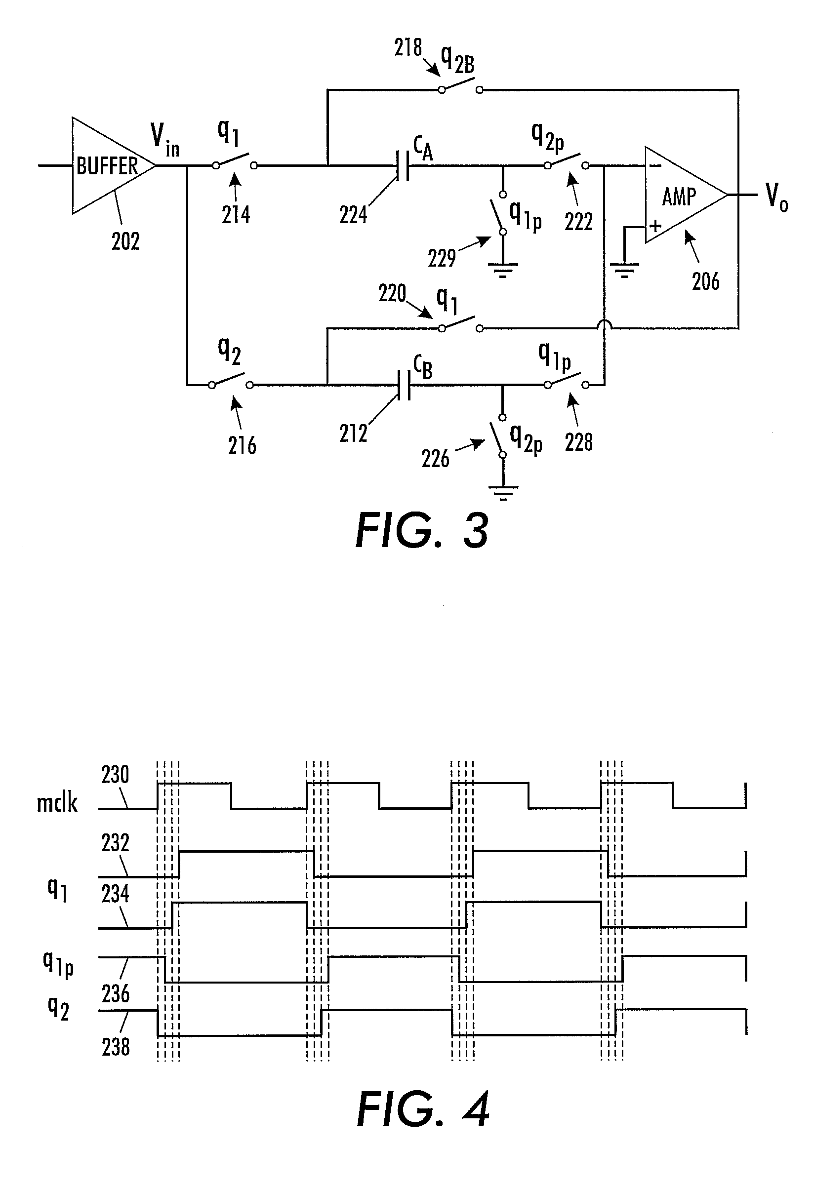
[0027]A sample and hold circuit uses two capacitors, charging one for a full cycle, while the other is connected to an output of an amplifier, and then switching the roles of the two capacitors. This allows a full cycle to charge the capacitor and hence reduce the current capability and hence power requirements by a factor of 2.

[0028]FIG. 3 illustrates sample and hold architecture using two sampling capacitors. The circuit contains a buffer 202 and a charge amp 206. The circuit also contains two charging capacitors 224 and 212 and switches 214, 216, 218, 220, 222, 226, 228, and 229.

[0029]These switches are c...


PUM


Abstract

A sample and hold circuit architecture samples using two capacitors that are cyclically switched between charge and discharge modes. The sample and hold circuit includes a buffer to receive an input signal to be sampled, a first sampling capacitor, a second sampling capacitor, and an amplifier. The first sampling capacitor is connected to the output of the buffer during the positive phase of a clock and across the feedback path of the amplifier during the zero phase of the clock. The second sampling capacitor is connected to the output of the buffer during the zero phase of the clock and across the feedback path of the amplifier during the positive phase of the clock. Neither the first sampling capacitor nor the second sampling capacitor is simultaneously connected to the buffer, the amplifier, or to each other.

Description

BACKGROUND AND SUMMARY[0001]Many modern electronic devices operate with one or more inputs as analog (continuously variable) signals. Since it is becoming more common for these devices to be digital in nature, it is necessary at some point to convert the analog signal to a sampled digital signal. A key part of this analog to digital conversion process is a sample and hold circuit.[0002]The sample and hold circuit is placed ahead of the circuit element or elements that do the actual conversion to digital values. Because the conversion takes a finite amount of time, it is necessary to provide the converter circuit with a stable, fixed, signal for the duration of the sampling time. The sample and hold circuit is the element that performs this operation. The sample and hold circuit consists of some sort of element that can sample the input signal for a short period of time, corresponding to the conversion time, and then provide this sampled value to the actual converter circuitry. The s...

Claims


Application Information

Patent Timeline
Patent Type & Authority Patents(United States)
IPC IPC(8): H03K5/00
CPCG11C27/026
Inventor AGHTAR, SAEED
Owner ANALOG DEVICES INC
Why Eureka
Try Eureka