Offset canceller for compensating for offset in signal output

a signal output and offset canceller technology, applied in the direction of differential amplifiers, amplifier details, amplifiers with semiconductor devices/discharge tubes, etc., can solve the problems of not being able to output signals during the operation of offset compensation, and the conventional offset canceller circuitry cannot be applicable, so as to achieve offset cancellation, uniform output voltage, and increase the effect of offset cancellation

Active Publication Date: 2008-09-09
LAPIS SEMICON CO LTD
View PDF8 Cites 7 Cited by
  • Summary
  • Abstract
  • Description
  • Claims
  • Application Information

AI Technical Summary

Benefits of technology

[0007]It is an object of the present invention to provide an offset canceller by means of which it is possible to output a signal in the course of the operation for offset compensation, and by means of which it is possible to compensate for the offset ascribable to the capacitance or resistance device externally connected to an operational amplifier.
[0011]According to the present invention, offset cancellation may sequentially be carried out while the outputting operation of the output circuits is continued. It is thus possible to obtain a uniform output voltage at all of the output terminals. It is also possible to raise the accuracy of the offset cancellation further by using finer divisions of the capacitances used for gain adjustment.
[0012]Moreover, the voltage follower, used in an LCD source driver, may be compensated for offset without employing capacitive devices. In addition, the offset cancellation may be carried out more accurately by raising the accuracy of the comparator and by employing finer divisions of the resistances used for providing variable resistances. In addition, signals may be output during the offset cancel operations.

Problems solved by technology

To such a case, the conventional offset canceller circuitry cannot be applicable.
Moreover, the conventional method for compensating for the offset suffers from the problem that no signal can be output during the operation of the offset compensation.

Method used


Image

  • Offset canceller for compensating for offset in signal output
  • Offset canceller for compensating for offset in signal output
  • Offset canceller for compensating for offset in signal output

Examples


Embodiment Construction

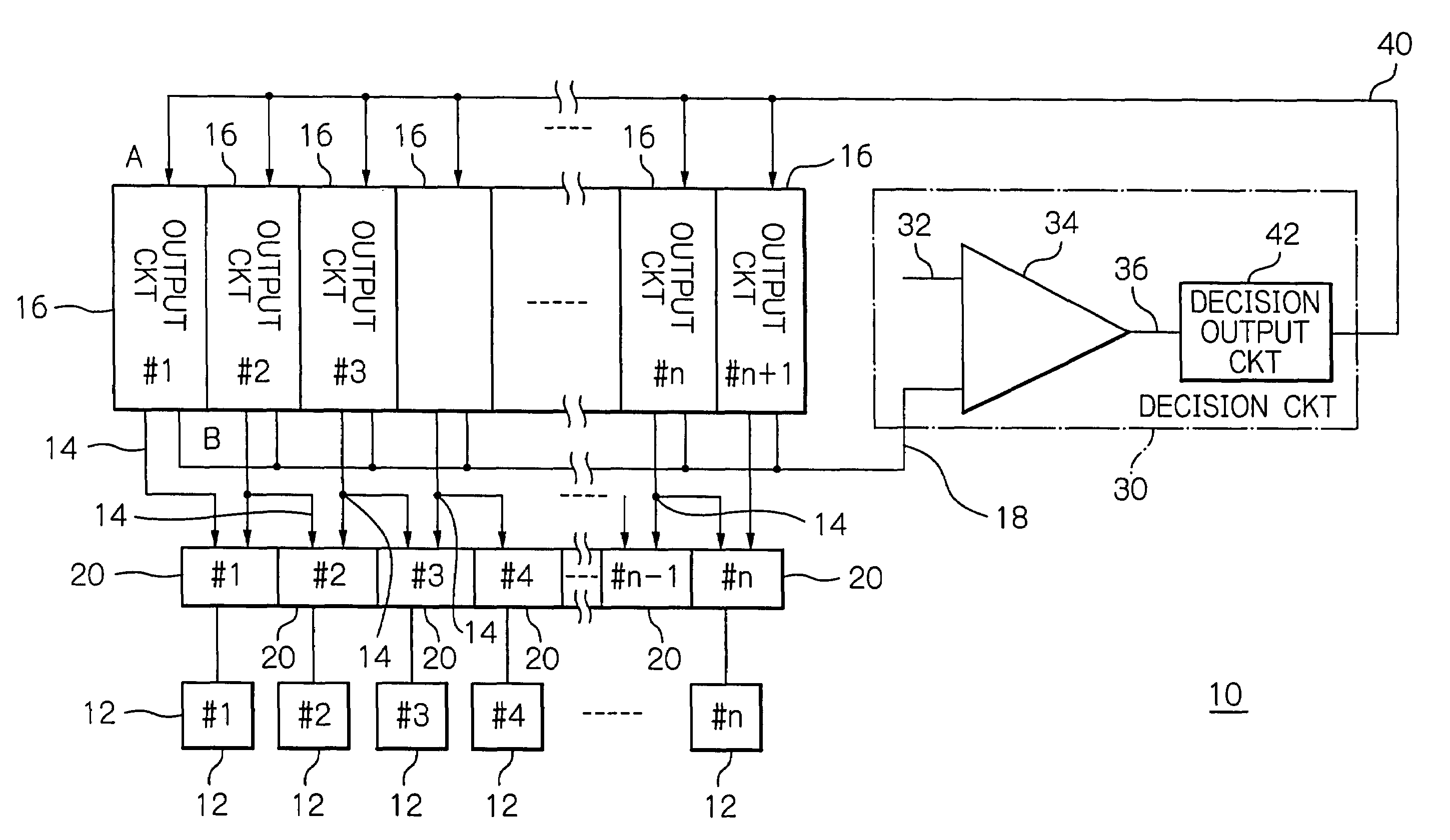
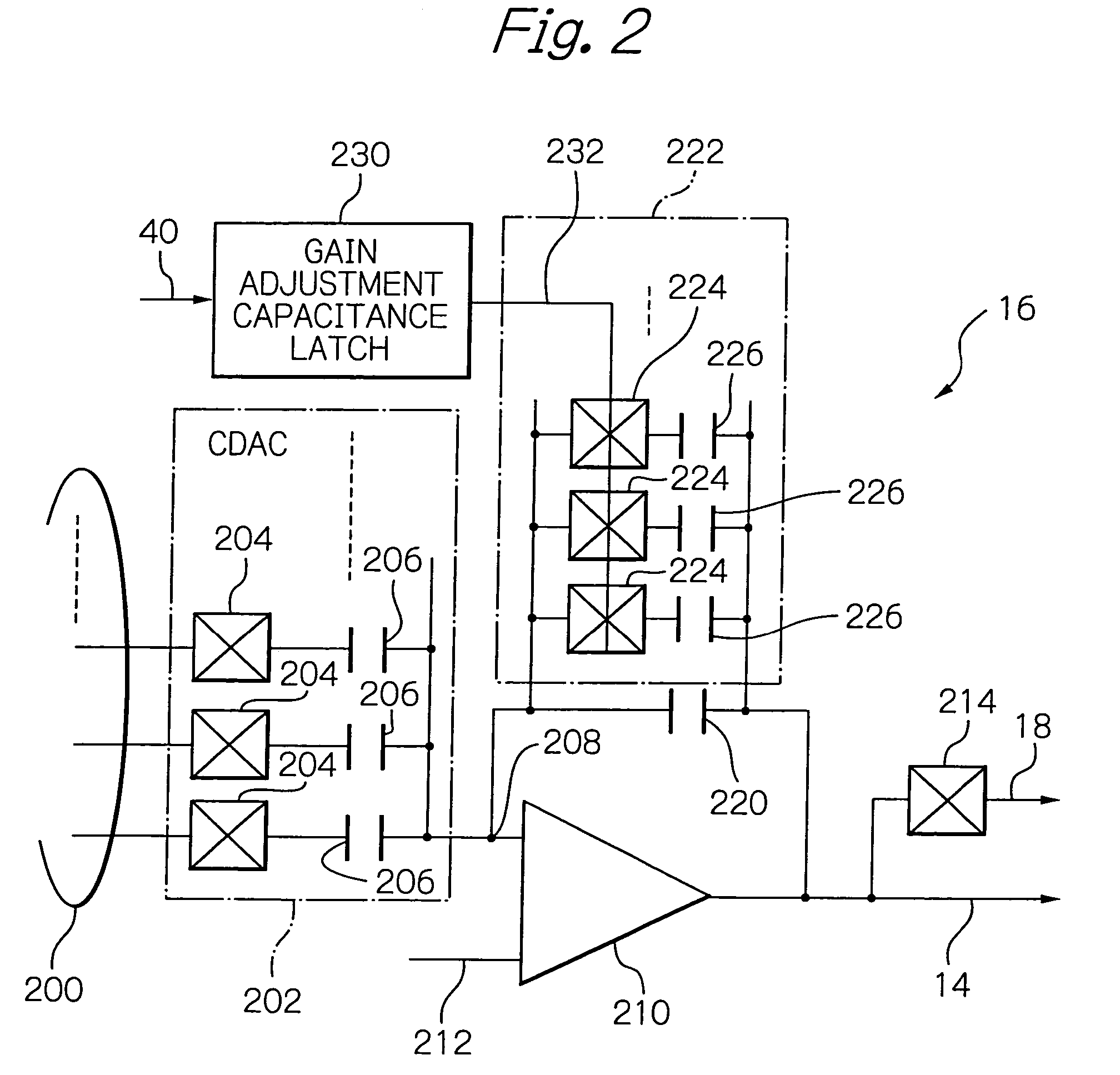
[0017]A preferred embodiment of an offset canceller according to the present invention will now be described in detail with reference the accompanying drawings. In FIG. 1, there is shown an embodiment of a driving circuit to which applied is the offset canceller of the present invention. In the following description, components not directly relevant to understanding the present invention will not be shown nor described.

[0018]A driving circuit 10 of the present embodiment is a liquid crystal device driver circuit for driving a liquid crystal display (LCD) device, for example. The driving circuit 10 includes a plural number of output circuits (#1 to #n+1) 16 each having its one outputl4 adapted for outputting a driving signal to associated one of a plural number of output terminals (#1 to #n) 12, where n denotes natural numbers. The output circuits (#1 to #n+l) 16 each output a driving signal on its other output 18. The outputs 14 of the output circuits (#1 to #n+1) 16 are connected t...


PUM


Abstract

An offset canceller outputs a signal during its offset compensating operation and compensates for the offset by capacitance or resistance devices connected externally to an operational amplifier. A driving circuit includes plural output circuits #1 to #n+1 for outputting driving signals to plural output terminals #1 to #n on one outputs and for outputting the driving signals on the other outputs coupled to corresponding plural output selectors #1 to #n, which then select one of two signals output from two neighboring output circuits to transmit the selected signals to the output terminals. The output circuits #1 to #n+1 have other outputs coupled to a decision circuit, which compares the signals to a reference voltage and outputs a decision signal representing the result of comparison at a predetermined timing. The output circuits execute the offset cancel operation responsive to the decision signal.

Description

BACKGROUND OF THE INVENTION[0001]1. Field of the Invention[0002]The present invention relates to an offset canceller for canceling the offset in a signal output. More particularly, the present invention relates to an offset canceller applicable to an output circuit of a liquid crystal display device driver having a plurality of output operational amplifiers, as an example.[0003]2. Description of the Background Art[0004]An integrated circuit for driving a liquid crystal display (LCD) device, for example, includes a plural number of output operational amplifiers. In canceling the offset of those operational amplifiers, the routine practice is to cancel only the offset voltage, as disclosed in, for example, U.S. Pat. Nos. 6,946,905 B2, 6,448,836 B2 and 6,930,529 B2 to Kokubun et al., Kokubun et al., and Tobita, respectively.[0005]However, if a capacitive or resistance device for setting the amplification factor is connected externally of the operational amplifiers, it is necessary to c...

Claims


Application Information

Patent Timeline
Patent Type & Authority Patents(United States)
IPC IPC(8): H03F1/02
CPCH03F3/45183H03F3/45475H03F3/45744H03F3/45968H03F3/45977H03F3/45753H03F2203/45728H03F2203/45616G09G3/20G09G3/36H03F1/30H03F3/45
Inventor HIGUCHI, KOJI
Owner LAPIS SEMICON CO LTD
Why Eureka
Try Eureka