Phase error detecting circuit and synchronization clock extraction circuit
a phase error detection and synchronization clock technology, applied in the field of phase error detection circuits, can solve problems such as narrow capture ranges, and achieve the effects of enhancing jitter, enhancing jitter, and expanding capture rang
- Summary
- Abstract
- Description
- Claims
- Application Information
AI Technical Summary
Benefits of technology
Problems solved by technology
Method used
Image
Examples
embodiment 1
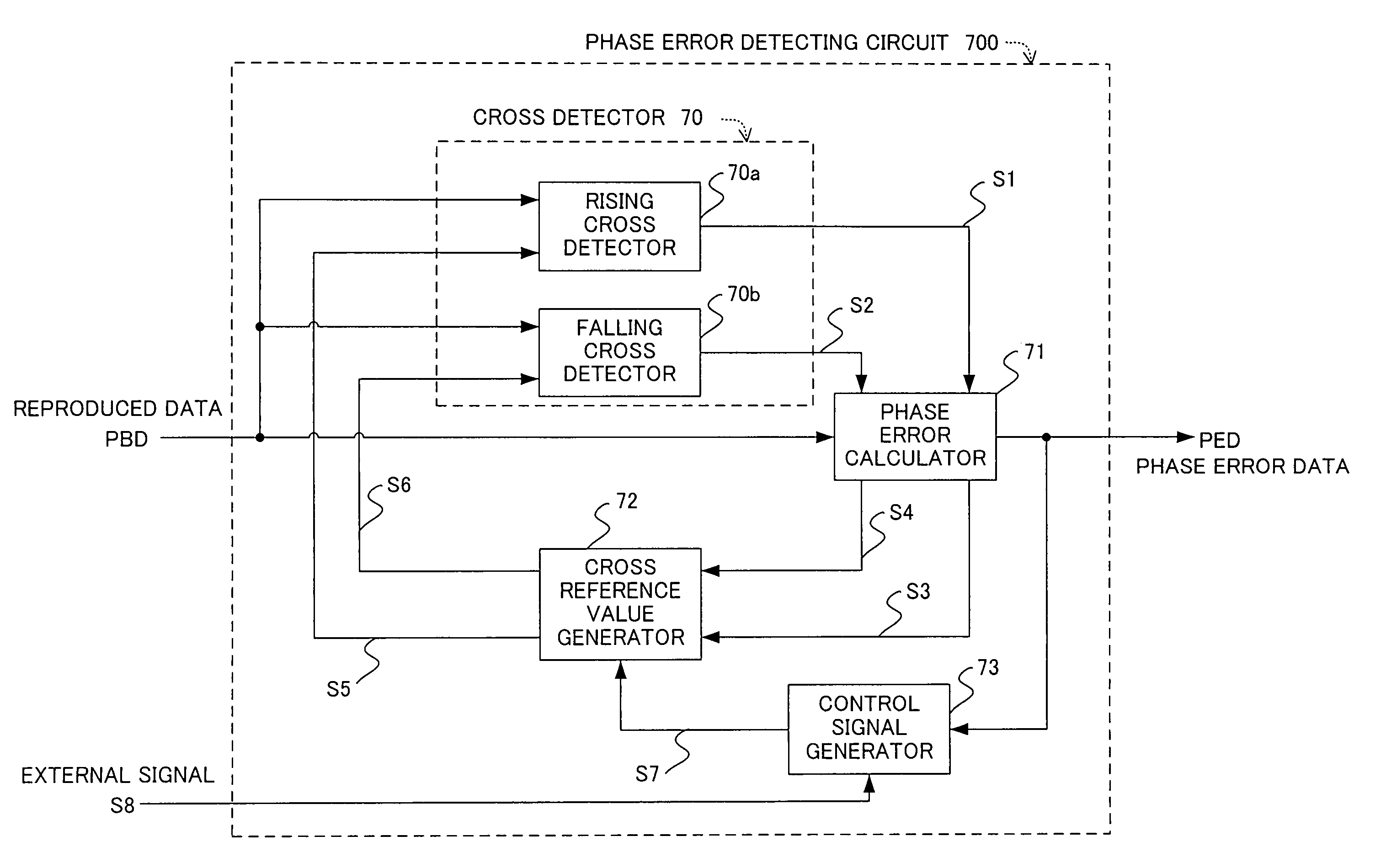
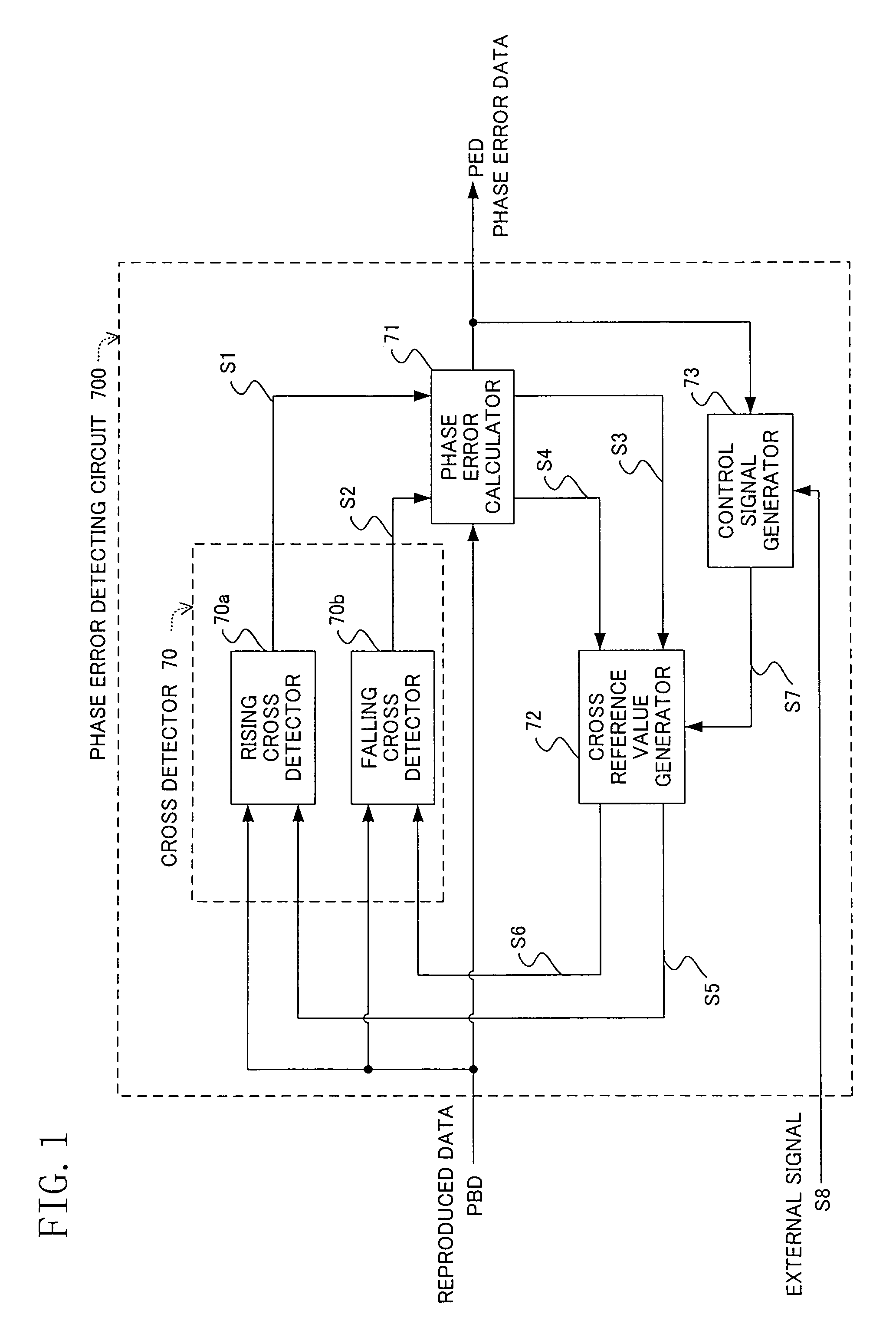
[0082]FIG. 1 shows a structure of a phase error detecting circuit as a first embodiment of the present invention. The phase error detecting circuit in the drawing is used as a replacement for the phase comparator 7 provided in the synchronous clock extracting circuit 13 of the digital signal processing circuit 12 in the reproduced signal processing circuit in the optical disk apparatus (record reproducing apparatus) shown in FIG. 23. Accordingly, the respective structures of the synchronous clock extracting circuit and the reproduced signal processing circuit each having the phase error detecting circuit are the same as in FIG. 23 so that the description thereof will be omitted.
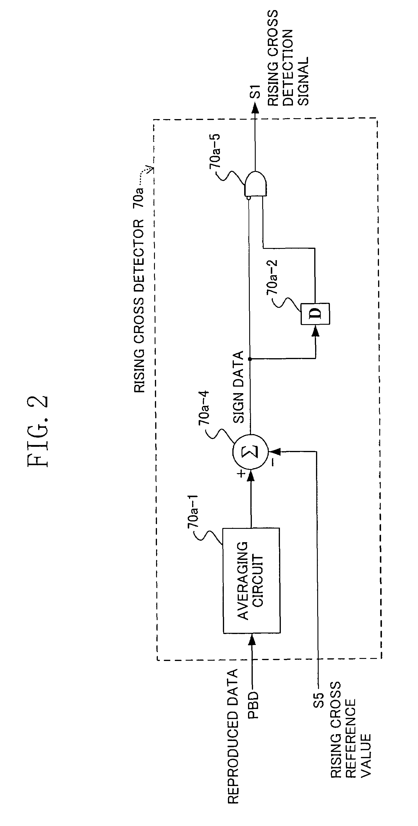
[0083]In FIG. 1, 700 is the phase error detecting circuit which detects a phase error from the reproduced data reproduced by the record reproducing apparatus and subjected to AD conversion (quantization) in the A / D converter 4 shown in FIG. 23 and outputs the detected phase error. The phase error detecting ci...
embodiment 2
[0098]A description will be given next to a phase error detecting circuit in the second embodiment. In the present embodiment, the cross reference value generator 72 generates a reference value different from that used in the first embodiment.
[0099]Specifically, the rising cross reference value S5 is outputted to the rising cross detector 70a and the rising cross reference value S5 having an equal absolute value and an inverted sign is outputted to the falling cross detector 70b, which will be described with reference to FIG. 6. The phase error data point PE3 upon the next rising is detected by using the level Lr at the phase error data point PE1 upon rising as the reference value and, for the detection of the phase error data points PE2 and PE4 upon falling, a value obtained by inverting the sign of the level Lr at the phase error data point PE1 upon rising is used as the reference value.
[0100]Accordingly, the capture range of the phase error detecting circuit can be enlarged in th...
embodiment 3
[0101]A description will be given next to a phase error detecting circuit according to the third embodiment. In the present embodiment, another embodiment of the generation of the reference value will be shown.
[0102]Specifically, the falling cross reference value S6 is outputted to the falling cross detector 70b by using the falling phase error data S4 inputted to the cross reference value generator 72, while the falling cross reference value S6 having an equal absolute value and an inverted sign is outputted to the rising cross detector 70a, which will be described with reference to FIG. 7. By using the level Lf at the phase error data point PE2 detected upon falling as the reference value, the phase error data point PE4 is detected upon the next falling and, for the detection of the phase error data point PE3 upon rising, a value obtained by inverting the sign of the level Lf at the phase error data point PE2 upon falling is used as the reference value.
[0103]Accordingly, the captu...
PUM
| Property | Measurement | Unit |
|---|---|---|
| frequency | aaaaa | aaaaa |
| phase error | aaaaa | aaaaa |
| phase error calculator | aaaaa | aaaaa |
Abstract
Description
Claims
Application Information


