Integrated circuit layout device, method thereof and program thereof

a technology of integrated circuits and layout devices, applied in the field of integrated circuit layout devices, a method and a program, can solve the problem that the timing error of each path cannot be improved in a short period of time, and achieve the effect of improving the timing error of each path and improving the timing error

Inactive Publication Date: 2008-09-09
FUJITSU LTD
View PDF13 Cites 217 Cited by
  • Summary
  • Abstract
  • Description
  • Claims
  • Application Information

AI Technical Summary

Benefits of technology

[0007]In the technologies described above, the timing error of the path was improved by executing only the SSTA, and the timing error of each path could not be improved in a short period of time. It is an object of the invention to improve the timing error of each path in a shorter period of time than by improving the timing error in a way that performs only the SSTA with respect to each of the paths of the integrated circuit.
[0008]The invention adopts the following means in order to solve the problems. (1) Namely, a layout device for an integrated circuit according to the invention (the layout device for the integrated circuit), comprises recording means recording connection information and delay information of wirings, timing value calculating means calculating a timing value with respect to each wiring path by a delay analysis of signal propagation based on the connection information and the delay information of the wirings, target value determining means determining a first target value serving as an improvement target of the wiring path, detecting means detecting an error wiring path exhibiting the timing value larger than the first target value, improving means changing the wiring connection so that the detected error wiring path shows a timing value smaller than the first target value, means updating the connection information and the delay information of the wirings, which are recorded in the recording means, into connection information and delay information of the wirings after changing the wiring connection, distribution calculating means calculating a first distribution about each wiring path by the delay analysis of the signal propagation based on the post-updating connection information and the post-updating delay information of the wirings, and a fluctuation factor, yield calculating means calculating a first yield of the integrated circuit from the first distribution, and judging means judging whether or not the first yield is within an allowable range of a predetermined value. With this configuration, it is possible to improve the timing error of the wiring path exhibiting the timing value larger than the target value for improving the timing error by the STA and the SSTA. Then, it is feasible to recognize whether the yield of the integrated circuit after improving the timing error of the wiring path falls within the allowable range of the predetermined value. Accordingly, the timing error of the wiring path can be improved in the shorter time than by improving the timing error of the wiring path in a way that executes only the SSTA.
[0009](2) The layout device for the integrated circuit may further comprise target value setting means setting a second target value used for determining the first target value, and predicting means predicting a second distribution from the first distribution when each wiring path attains the second target value, wherein the yield calculating means may calculate a second yield of the integrated circuit from the second distribution, and the target value determining means may determine the second target value as the first target value when the second yield is within the allowable range of the predetermined value. With this configuration, it is possible to recognize whether the yield of the integrated circuit after improving the timing error falls within the allowable range of the predetermined value. Accordingly, a necessity of actually conducting the SSTA is eliminated, and the timing error of the wiring path can be improved in the short time.
[0010](3) In the layout device for the integrated circuit, the judging means may judge whether or not the first yield takes, if the second yield is not the allowable range of the predetermined value, a value smaller than the predetermined value, the target value setting means may set, when the second yield takes the value smaller than the predetermined value, a value smaller than the second target value newly as the second target value, and may set, when the second yield does not take the value smaller than the predetermined value, a value larger than the second target value newly as the second target value, and the layout device may further comprise control means controlling the yield calculating means, the judging means, the target value determining means, the target value setting means and the predicting means to perform repetitive executions till the second yield falls within the allowable range of the predetermined value. With this configuration, the target value serving as a target for improving the timing error can be surely determined.
[0011](4) In the layout device for the integrated circuit, the timing value calculating means may calculate a timing value about each wiring path by the delay analysis of the signal propagation based on the connection information and the delay information of the wirings after changing the connections of the wirings; and the layout device further comprises a means determining a specified wiring path based on the timing value, the timing value calculated a timing value about each wiring path by the delay analysis of the signal propagation based on the connection information and the delay information of the wirings after changing the connections of the wirings by said timing value calculating means, wherein said distribution calculating means calculates the first distribution about the specified wiring path by the delay analysis of the signal propagation based on the post-updating connection information, the post-updating delay information and the fluctuation factor. This configuration makes it possible to specify the wiring path exhibiting the large timing error that affects the yield of the integrated circuit. It is therefore possible to reduce the processing time of the SSTA by conducting the SSTA about only the specified wiring path.
[0014]According to the invention, it is possible to improve the timing error of each path in a shorter period of time than by improving the timing error in a way that performs only the SSTA with respect to each of the paths of the integrated circuit.

Problems solved by technology

In the technologies described above, the timing error of the path was improved by executing only the SSTA, and the timing error of each path could not be improved in a short period of time.

Method used


Image

  • Integrated circuit layout device, method thereof and program thereof
  • Integrated circuit layout device, method thereof and program thereof
  • Integrated circuit layout device, method thereof and program thereof

Examples


first embodiment

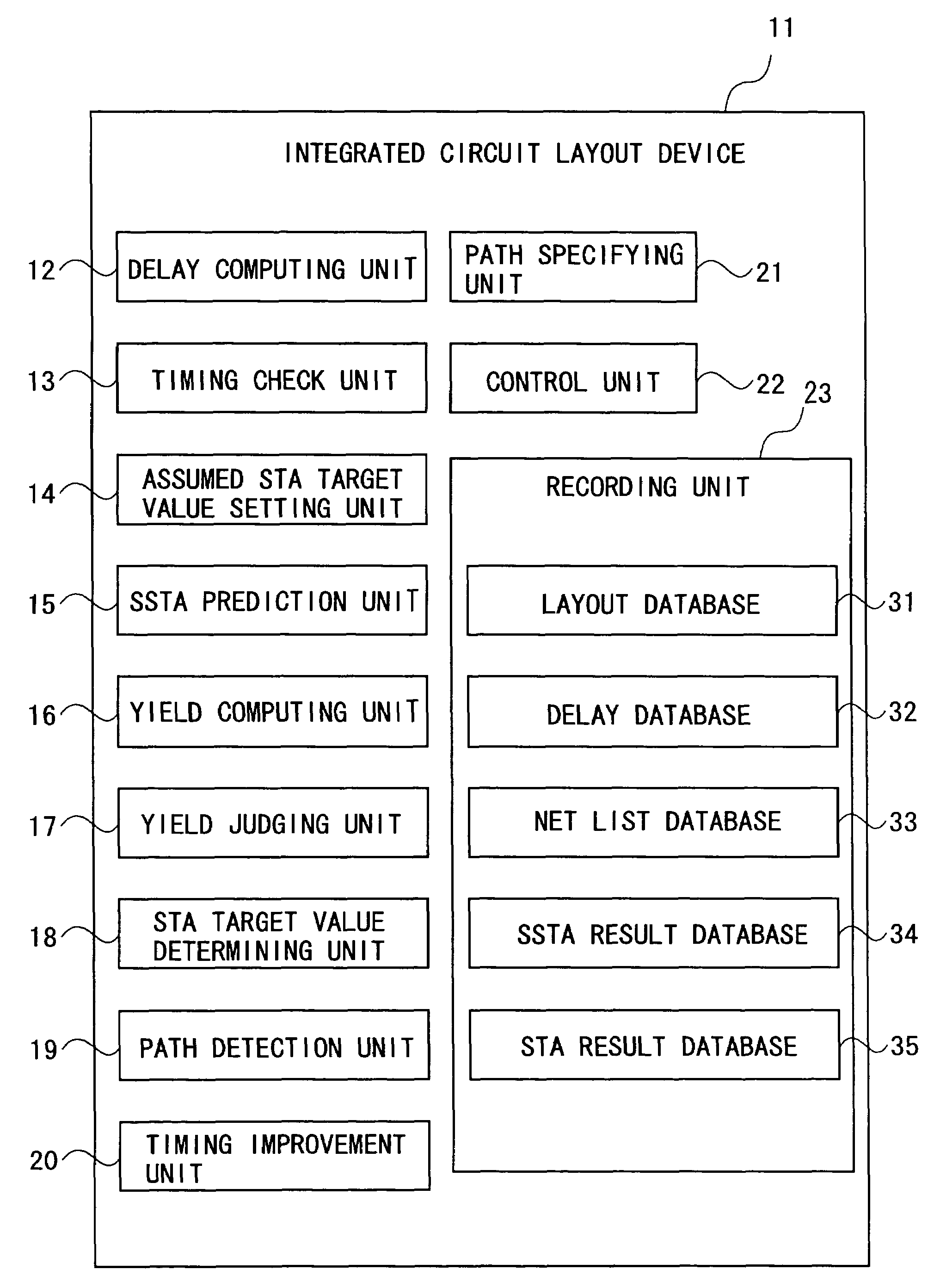
[0050]FIG. 7 is a flowchart of a process of converging the yield of the integrated circuit within a yield target allowable range. To start with, the delay computing unit 12 computes the delay time of each path on the basis of the layout information and the wiring information of the target integrated circuit. The layout information and the wiring information of the target integrated circuit are previously recorded on the layout database 31. Then, the delay computing unit 12 records the delay database 32 with the delay information defined as a result of performing the delay computation (S701).

[0051]Next, based on the net list and the delay information, the timing check unit 13 executes the timing check by the SSTA and the STA with respect to each of the paths of the target integrated circuit (S702). Herein, the timing check may involve doing simulation and may also involve making the actual measurement. Further, the timing check unit 13 records a result of performing the timing check ...

second embodiment

[0075]The first embodiment is that in the check value distribution predicting process, the check value distribution is parallel-shifted in the smaller check value direction by the value obtained by subtracting the assumed STA target value from the check value of each of the paths of the target integrated circuit. A second embodiment is that the parallel-shifting value is adjusted by a coefficient in a way that uses an empirically experimentally acquired coefficient. In this case, the coefficient can be changed on a path-by-path basis from a circuit topology such as path branching and path confluence. Further, in the check value distribution predicting process, the post-prediction check value distribution can be also obtained not by parallel-shifting the check value distribution but by changing a form of the check value distribution. In this case, the post-prediction check value distribution can be also acquired by changing the form of the check value distribution from the circuit to...


PUM


Abstract

A layout device for an integrated circuit executes calculating a timing value with respect to each wiring path by a analysis based on connection information and delay information of wirings, determining a target value serving as an improvement target of the wiring path, detecting an error wiring path exhibiting the timing value larger than the target value, changing the wiring connection so that the error wiring path shows a timing value smaller than the target value, updating these piece of information into connection information and delay information of the wirings after changing the wiring connection, calculating a distribution about each wiring path by the analysis based on the post-updating connection information and the post-updating delay information of the wirings and a fluctuation factor, calculating a yield of the integrated circuit from the distribution, and judging whether or not the yield is within an allowable range of a predetermined value.

Description

BACKGROUND OF THE INVENTION[0001]The invention relates to an integrated circuit layout device, a method thereof and a program thereof.[0002]In designing the integrated circuit (e.g., an LSI (Large Scale Integration), an IC (Integrated Circuit), etc) a static timing analysis (Static Timing Analysis) has hitherto been carried out. The static timing analysis (which will hereinafter also be abbreviated to STA) is that a delay of a path is basically computed in total of maximum values or minimum values of delay values of signal propagation time of each of elements building up a logic circuit that connects one sequential circuit to another sequential circuit, and the timing analysis is thus performed. At the present, however, a scatter in the respective element (a manufacturing scatter) becomes relatively large as compared with a delay constraint value of the path. Then, it is difficult to make a design satisfying a timing constraint in the total of the maximum values (or the minimum valu...

Claims


Application Information

Patent Timeline
Patent Type & Authority Patents(United States)
IPC IPC(8): G06F17/50
CPCG06F17/5031G06F30/3312
Inventor IKEDA, HIROSHI
Owner FUJITSU LTD
Why Eureka
Try Eureka