Capacitive/resistive devices, organic dielectric laminates and printed wiring boards incorporating such devices, and methods of making thereof

a technology of resistors and capacitors, applied in the direction of printed resistors, printed capacitors, printed circuit non-printed electric components, etc., can solve the problems of increasing fabrication costs and reliability reduction of solder joints, so as to reduce the cost and difficulty of creating resistors and capacitor functions, improve reliability, and free valuable real estate

Active Publication Date: 2008-09-30
CHEMTRON RES
View PDF29 Cites 3 Cited by
  • Summary
  • Abstract
  • Description
  • Claims
  • Application Information

AI Technical Summary

Benefits of technology

[0006]According to the above embodiment, both the resistor and the capacitor functions may be integrated into a single buried laminate, reducing the cost and difficulty in creating the resistor and capacitor functions. When the capacitive / resistive device is incorporated in a printed wiring board, embedding the capacitive / resistive device also frees up valuable real estate. Further, solder joints associated with SMT devices may be eliminated, thereby improving reliability. The capacitive / resistive device can be processed using conventional etching processes, further reducing production costs.

Problems solved by technology

Further, the requirement for solder joints reduces reliability and increases costs of fabrication.

Method used


Image

  • Capacitive/resistive devices, organic dielectric laminates and printed wiring boards incorporating such devices, and methods of making thereof
  • Capacitive/resistive devices, organic dielectric laminates and printed wiring boards incorporating such devices, and methods of making thereof
  • Capacitive/resistive devices, organic dielectric laminates and printed wiring boards incorporating such devices, and methods of making thereof

Examples


example

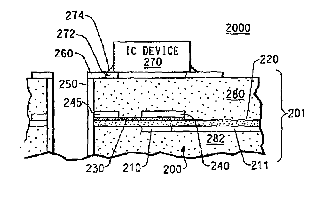
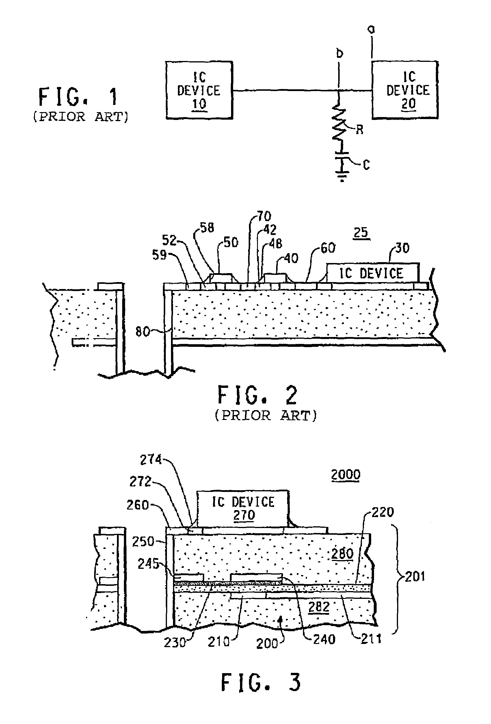
[0024]This example of the device 200 is discussed with reference to FIG. 3. In this example, the electrodes 210, 240 are formed from copper foils. Resistive material 230 is a plated nickel phosphorus alloy of sheet resistivity 50 ohms per square. The dielectric 220 is an unfilled polyimide dielectric (INTERRA™ HK 04, available from DuPont Electronic Technologies, Wilmington, Del.) of 25 microns thickness having a dielectric constant of 3.5 thereby giving a capacitance density of 800 picoFarads per square inch.

[0025]The size (when viewed from a top plan perspective) of the capacitor needed for a transmission line termination of 30 picoFarad is 24.2 square mm, which corresponds to slightly less than 5 mm by 5 mm.

[0026]The size of the resistor in this example for a nominal 60 ohm resistance can be varied, as long as the length to width ratio is maintained at 1.2 to 1.0. The above capacitor is easy to make to relatively high tolerances.

[0027]According to the above embodiment, thin capac...


PUM

PropertyMeasurementUnit
impedanceaaaaaaaaaa
dielectric constantaaaaaaaaaa
thicknessaaaaaaaaaa

Abstract

This invention relates to a capacitive / resistive device, which may be embedded within a layer of a printed wiring board. Embedding the device conserves board surface real estate, and reduces the number of solder connections, thereby increasing reliability. More specifically, the device, comprises a first metallic foil; a second metallic foil; a first electrode formed from the first metallic foil; a dielectric disposed over the first electrode, a resistor element formed on and adjacent to the dielectric; a conductive trace; and a second electrode formed from the second metallic foil and disposed over the dielectric and in electrical contact with the resistor element, wherein the dielectric is disposed between the first electrode and the second electrode and wherein said dielectric comprises an unfilled polymer of dielectric constant less than 4.0. This invention also relates to a method of making the device.

Description

BACKGROUND[0001]The technical field relates to devices having both a capacitive and resistive functions, and methods of incorporating such devices in organic dielectric laminates and printed wiring boards.[0002]Capacitors and resistors may be used in series for transmission line termination of signal traces extending between integrated circuit (IC) devices. The capacitors and resistors are used to match the impedance of an IC device to a line, or to reduce or eliminate signal reflection. Some circuits are continuous load and use a resistor in parallel with the line. Non-continuous load circuits have a resistor and capacitor in series and are useful for low power ICs. FIG. 1 schematically illustrates a non-continuous load termination of IC devices 10 and 20.[0003]In FIG. 1, the distance from a to b is typically short. The value of the resistor R is chosen to match the line impedance and is typically about 45-80 ohms. The value of the capacitor C is chosen so that the RC time constant...

Claims


Application Information

Patent Timeline
Patent Type & Authority Patents(United States)
IPC IPC(8): H05K1/16
CPCH05K1/162H05K1/167H05K3/429H05K2201/0154H05K2201/0355Y10T29/435H05K2201/09672H05K2201/09763H05K2203/0361H05K2203/1461H05K2201/09309H05K1/16
Inventor BORLAND, WILLIAM J.COX, G. SIDNEYMCGREGOR, DAVID ROSS
Owner CHEMTRON RES
Why Eureka
Try Eureka