
Dielectric-filled transmission lines

a technology of dielectric filling and transmission lines, applied in the field of electric conductors, can solve the problems of increasing complexity and density of circuit boards, affecting the development of circuit boards, and affecting the electrical properties of lines, so as to reduce dielectric loss, and reduce the loss of dielectrics.

Inactive Publication Date: 2008-10-07
RPX CLEARINGHOUSE
View PDF2 Cites 4 Cited by
  • Summary
  • Abstract
  • Description
  • Claims
  • Application Information

AI Technical Summary

Benefits of technology

[0003]In accordance with the present invention a printed circuit board transmission line has an outer conductive wall surrounding an inner dielectric core. The outer conductive wall may be formed by joining multiple transmission line traces into a single transmission line of rectangular cross-section. The resulting transmission line has a greater conductive surface area for a given area of substrate than a standard conductive trace, and hence mitigates loss due to skin effect. The interior dielectric portion can reduce dielectric loss associated with induced magnetic fields. Dielectric-core transmission lines may be disposed both within inner layers of printed circuit boards and on outer layers of printed circuit boards.
[0004]In an alternative embodiment, the dielectric-core transmission line is disposed inside a grounded shielding to provide a form of coaxial conductor that mitigates cross talk from adjacent transmission lines and EMI. The shielding may include a dielectric portion disposed within an outer metallic wall, both of which are disposed around the dielectric-core transmission line.
[0007]The edge-coupled and broadside coupled configurations provide common noise rejection. However, because of limitations associated with printed circuit board geometry including layer thickness and trace thickness it may not be practical to form the walls of the transmission lines which are orthogonal with a plane defined by a layer of the printed circuit board with as great a width as the walls of the transmission lines which are parallel with that plane. Consequently, broadside-coupled differential pairs may have a greater coupled surface area relative to edge-coupled differential pairs, e.g., by a ratio of 8:1. The relatively greater coupled surface area results in a relatively cleaner signal transmission. Further, the broadside-coupled configuration occupies less area on a substrate than an edge-coupled configuration with similarly sized transmission lines. However, the relatively greater coupled surface area and thicker substrate may also result in relatively greater signal attenuation per unit length. Those skilled in the art will recognize how to use these different advantages to achieve a desired result for a specific implementation.
[0009]One aspect of the invention is a method for manufacturing the dielectric-core transmission lines and shielding. To form a single-ended dielectric-core transmission line an intermediate layer having an intermediate conductive trace on a substrate is disposed above a lower, ground layer. An upper signal layer having an upper conductive trace of lesser width than the intermediate conductive trace is disposed over the intermediate layer such that the upper conductive trace is substantially centered over the intermediate conductive trace. Note that the upper and intermediate conductive traces are now separated by a dielectric. A controlled-depth laser cut or mechanical mill is then made along both edges of the upper conductive trace. In particular, trenches reaching to the intermediate conductive trace are formed on either side of the upper conductive trace. Sidewalls connecting the upper and intermediate conductive traces are then formed in the trenches by filling the trenches with conductive paste or other conductive material, or alternatively by electro-less or electroplate deposition of a conductive material such as copper. It should be noted that the relatively lesser width of the upper conductive trace facilitates formation of the trenches and sidewalls by enabling trench formation in a plane orthogonal with the plane defined by a layer of the printed circuit board. Hence, the laser or mechanical milling bit may be situated perpendicular to the top and bottom of the printed circuit board and the relative difference in ablation properties between the substrate and the intermediate conductive trace may be used to advantage.

Problems solved by technology

In the case of printed circuit boards, this trend has prompted development of circuit boards with ever-increasing complexity and density.
While this is beneficial to increasing the density of the circuitry the lines are becoming so small that their electrical properties are an impediment for certain applications.
For example, cross-talk between closely spaced transmission lines is an impediment to high data rate transmission applications.
Similarly, electromagnetic interference (“EMI”) can be a problem for high data rate transmission.
Resistive and dielectric losses associated with “skin effect” and transmission line length in relatively narrow conductive traces are also problematic.

Method used


Image

  • Dielectric-filled transmission lines
  • Dielectric-filled transmission lines
  • Dielectric-filled transmission lines

Examples


Embodiment Construction

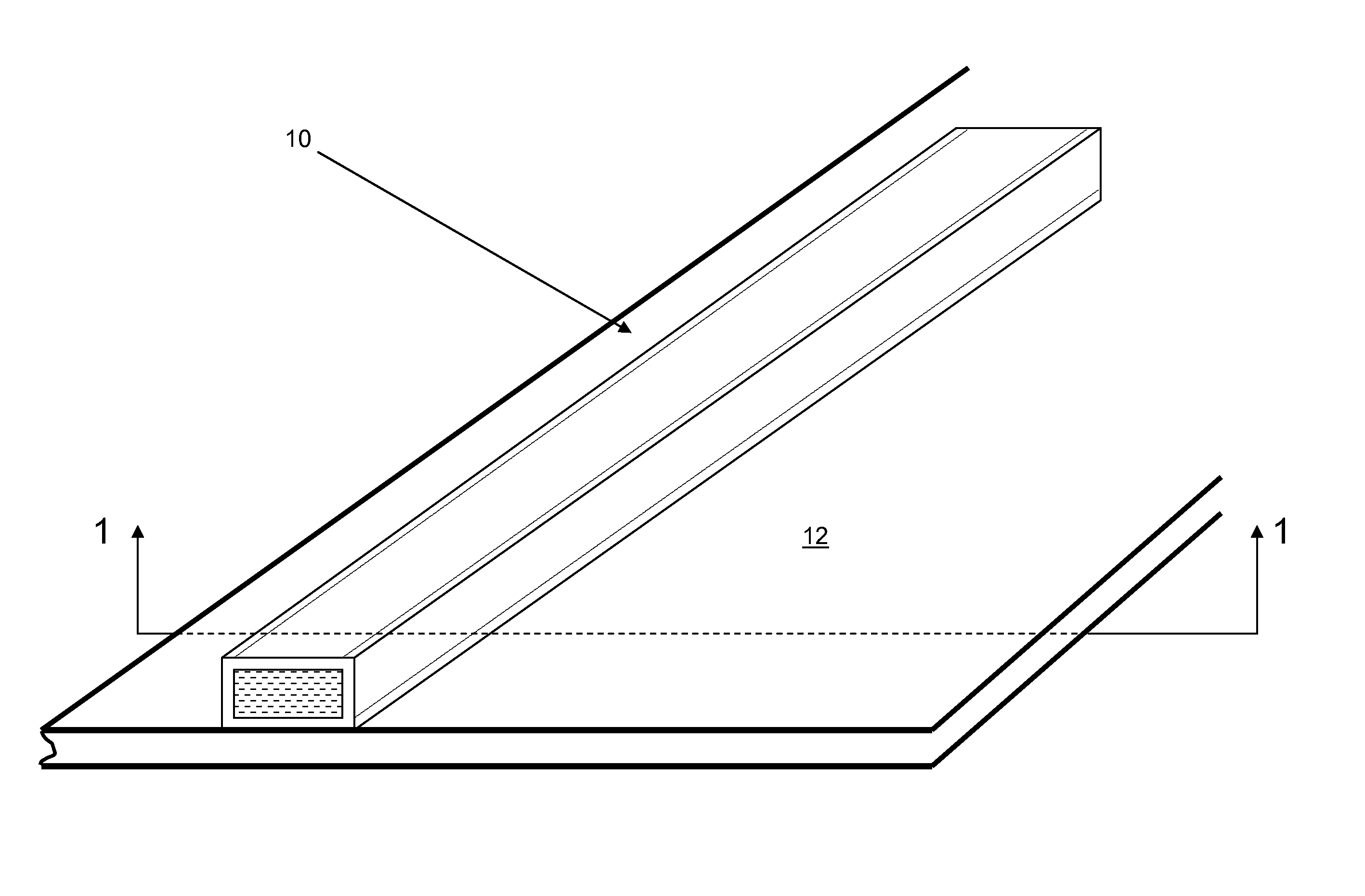
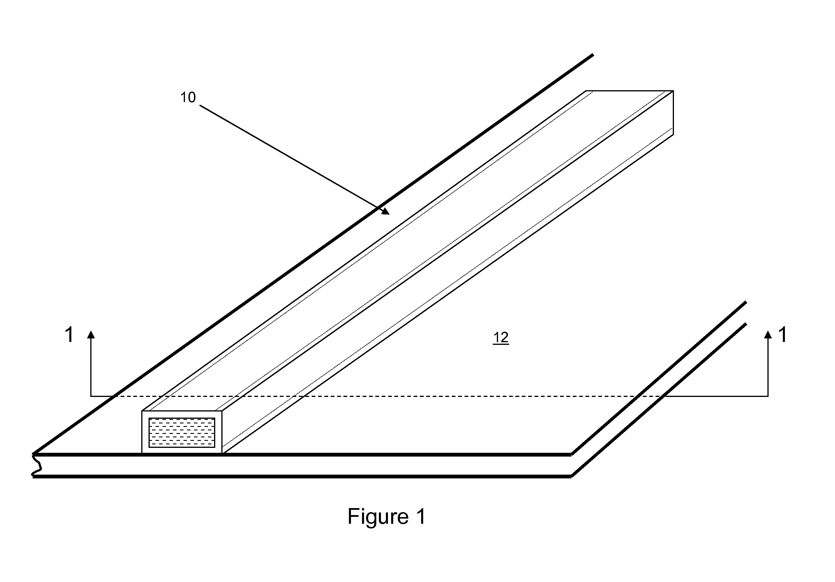
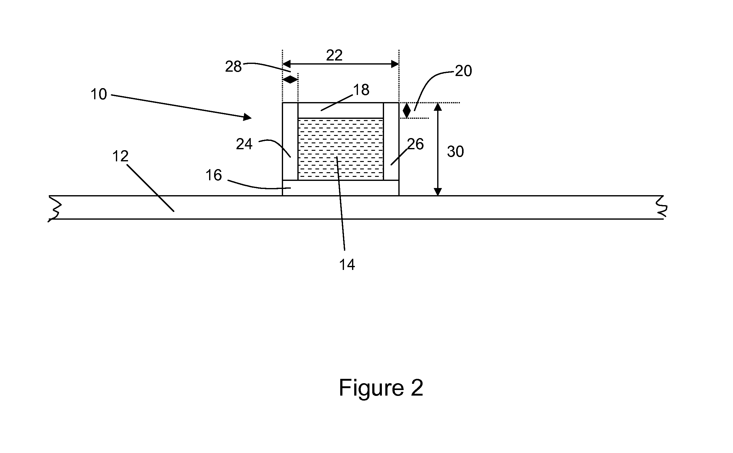
[0022]Referring to FIGS. 1 and 2, a printed circuit board transmission line 10 disposed on a substrate 12 has a tube-like outer conductive wall surrounding an inner dielectric core 14 (see FIG. 4). As seen in FIG. 2, the outer conductive wall includes four conductive sidewalls 16, 18, 24, 26 which are connected to form a continuous, uninterrupted structure having a rectangular cross-section. It should be noted however that other cross-sectional geometries including but not limited to triangular, circular, and any four-sided structure may be employed. First and second ones of the sidewalls 16, 18 are formed from copper or other electrically conductive material in a manner known for formation of conductive traces on a substrate layer of a printed circuit board. Further, the first and second sidewalls may have a thickness 20 similar to known conductive traces, such as 10-25 microns. The conductive wall has a width 22 similar to known conductive traces, such as 50-400 microns. Third and...


PUM


Abstract

A printed circuit board transmission line has an outer conductive wall surrounding an inner dielectric core. The transmission line may be disposed inside a grounded shielding to provide a form of coaxial conductor that mitigates cross talk from adjacent transmission lines and EMI. Further, groups of dielectric-core transmission lines may be disposed within a single grounded shield. For example, edge coupled differential pairs may be disposed in parallel with each other on a plane defined by a layer of the printed circuit board, i.e., side-by-side. Further, broadside-coupled differential pairs of dielectric-core transmission lines may be disposed in parallel with each other in a stack which is orthogonal with the plane defined by a layer of the printed circuit board, i.e., one on top of the other. Further, a plurality of dielectric-core transmission lines which may include all or ones of single-ended lines and differential pairs may be disposed within a single grounded shield.

Description

FIELD OF THE INVENTION[0001]This invention is generally related to electrical conductors, and more particularly to electrical conductors on printed circuit boards.BACKGROUND OF THE INVENTION[0002]It is generally desirable to provide electronic products in the smallest practical size. Consequently, there is a long term development trend of reducing the size of various electronic components such as integrated circuits, passive components, power supplies, and printed circuit boards. In the case of printed circuit boards, this trend has prompted development of circuit boards with ever-increasing complexity and density. Increases in density are typically associated with reduction of both the width of transmission lines and the separation between transmission lines to the extent practical with existing manufacturing technology. Current manufacturing techniques enable reliable production of printed circuit board with very small transmission lines. While this is beneficial to increasing the...

Claims


Application Information

Patent Timeline
Patent Type & Authority Patents(United States)
IPC IPC(8): H01P3/08
CPCH01P3/06H01P5/183H05K1/0221H05K1/024H05K2201/09672H05K2201/09809H05K2201/09981
Inventor KWONG, HERMANWYRZYKOWSKA, ANETAMARCANTI, LARRY
Owner RPX CLEARINGHOUSE
Learn More