Semiconductor laser device and method for fabricating the same

a laser device and semiconductor technology, applied in semiconductor lasers, laser details, electrical equipment, etc., can solve the problems of increasing waveguide loss, increasing waveguide loss, and reducing the reproducibility of laser devices, so as to achieve small threshold-value variation, large threshold-value variation, and high reproducibility

Active Publication Date: 2008-10-07
PANASONIC SEMICON SOLUTIONS CO LTD
View PDF6 Cites 2 Cited by
  • Summary
  • Abstract
  • Description
  • Claims
  • Application Information

AI Technical Summary

Benefits of technology

[0017]A saturable absorber is generally formed in an active layer. In this case, light distribution of guided light propagating in a waveguide is laterally extended to an active layer formed under a current blocking layer so that the saturable absorber is formed in the active layer. This active layer region initially serves as an absorber to laser light. However, as a result of electron-hole pair generation in the active layer due to excitation by the laser light itself, light absorption is reduced. The reduction of light absorption reduces a waveguide loss, so that light power increases and excitation of the electron-hole pairs are promoted in the active layer region. Accordingly, the light absorption is further reduced and, consequently, the saturable absorber becomes transparent to laser light. As a result, light power rapidly increases. That is, light power pulses and increases. When light power increases in this manner, the excited electron-hole pairs are lost by recombination due to induced emission, so that the active layer region in which the saturable absorber is formed functions as an absorber again. As a result, self-oscillation in which light power pulses and vibrates with time is obtained.
[0049]As described above, according to the present invention, in a semiconductor laser device in which a plurality of light-emitting elements emitting light with different wavelengths are integrated on the same substrate, e.g., in a two-wavelength semiconductor laser device in red and infrared regions, ΔN (the effective refractive-index difference between the inside and outside a current injection stripe) i.e., the shape of light distribution, is allowed to be precisely controlled without decrease of a COD (melt fracture) level and degradation of efficiency in utilizing light in an optical system. Accordingly, a multiple-wavelength semiconductor laser device which has a low-noise characteristic with self-oscillation and in which no heat saturation occurs even under a high temperature of, for example, about 85° C. is achieved.

Problems solved by technology

However, formation of a saturable absorber leads to an increase of a waveguide loss.
As a result, a light power of 5 mW, which is necessary for playback of an optical disk, is not obtained.
In a structure in which a saturable absorber is formed in an active layer, if light distribution is excessively extended in the horizontal / lateral direction, the volume of the saturable absorber increases and a waveguide loss increases, thus leading to an increase of the operation current value and heat saturation of light power during high-temperature operation.
As a result, a low-noise characteristic is impaired.

Method used


Image

  • Semiconductor laser device and method for fabricating the same
  • Semiconductor laser device and method for fabricating the same
  • Semiconductor laser device and method for fabricating the same

Examples


Embodiment Construction

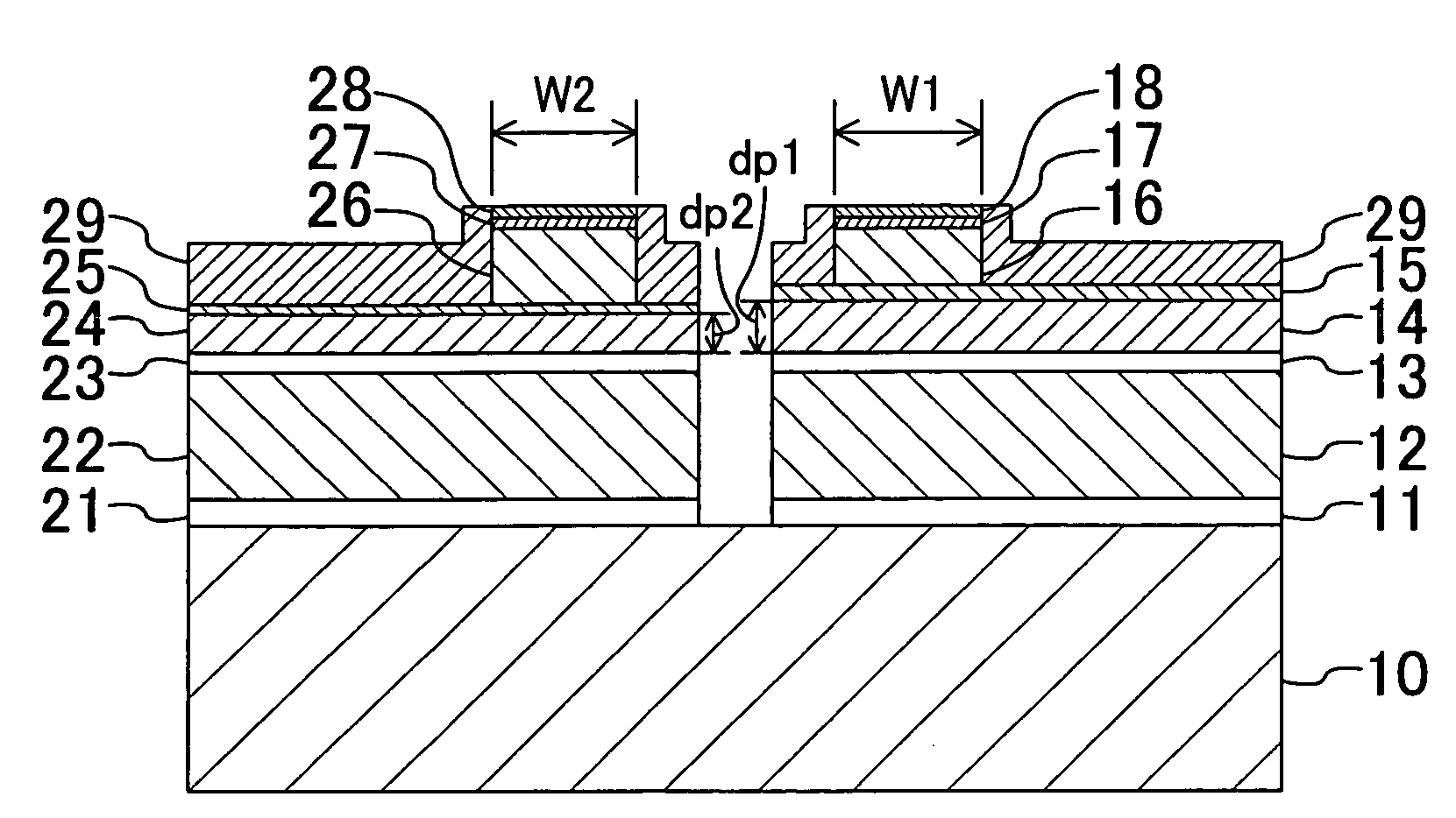
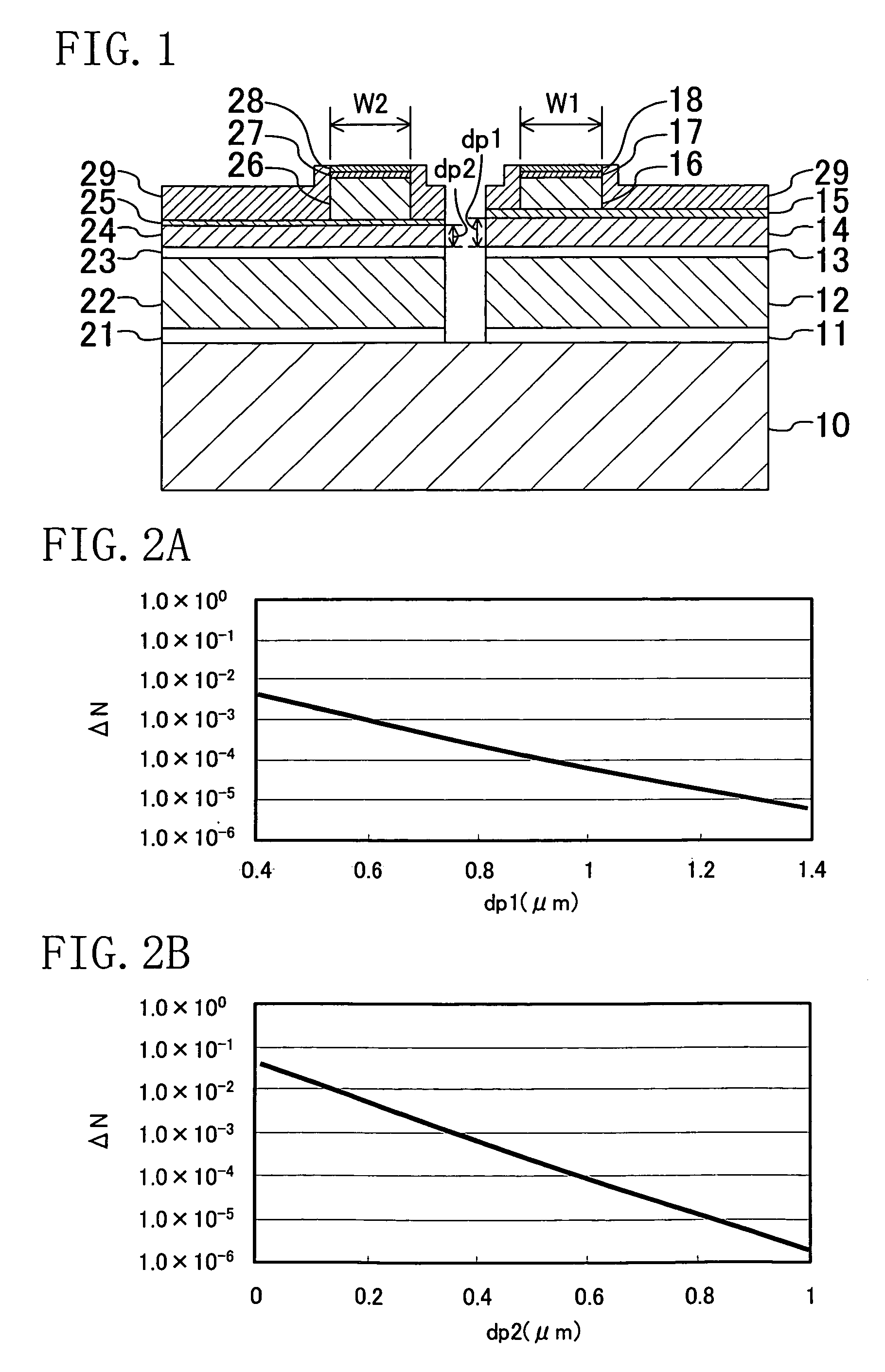
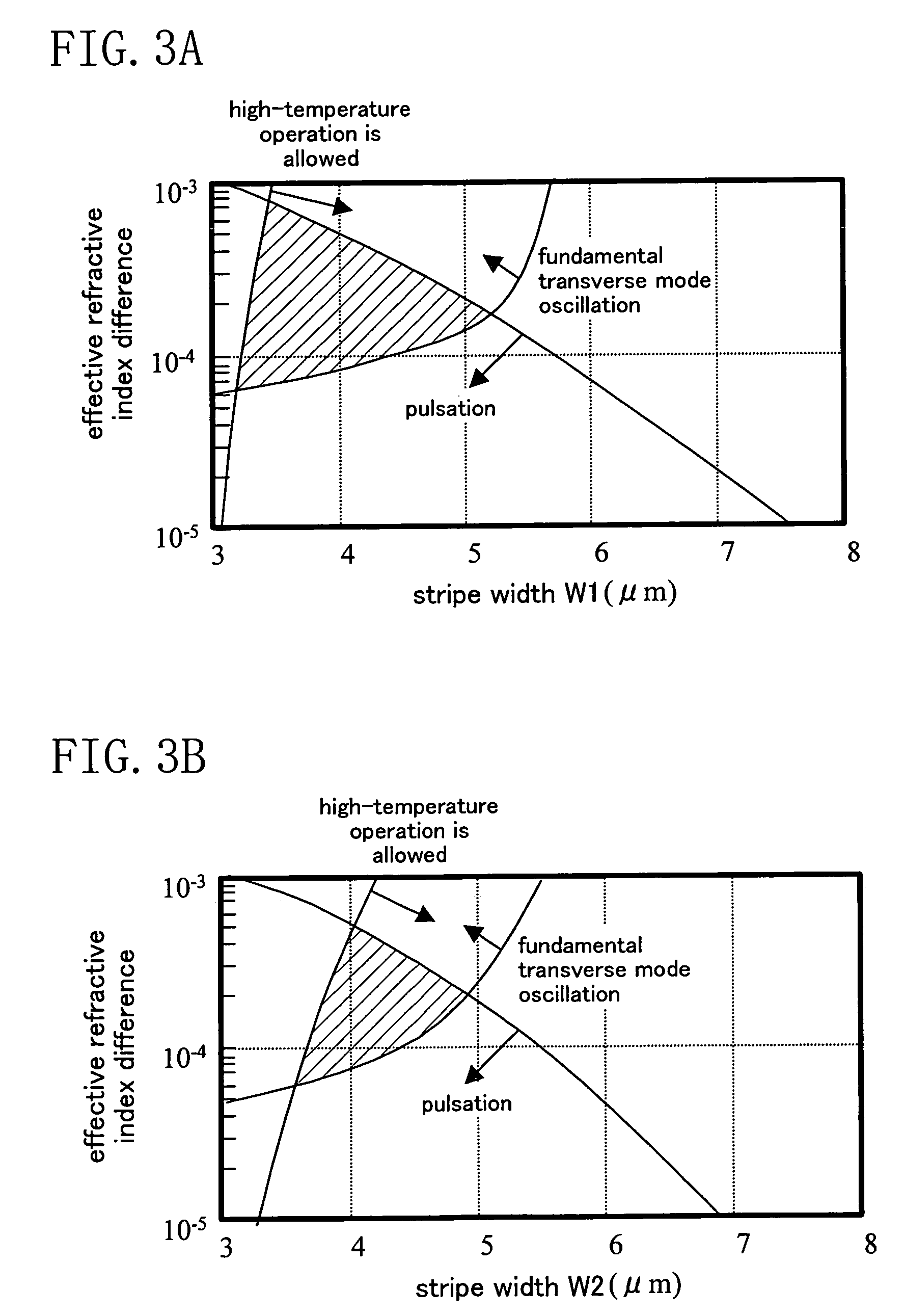
[0063]Hereinafter, a semiconductor laser device and a method for fabricating the device according an embodiment of the present invention will be described with reference to the drawings.

[0064]FIG. 1 is a cross-sectional view schematically illustrating a structure of a semiconductor laser device according to an embodiment of the present invention. In the structure illustrated in FIG. 1, a red laser and an infrared laser are integrated on an n-type GaAs substrate 10 whose principal plane is inclined with respect to the (100) plane toward the [011] direction at 10°, for example.

[0065]First, a structure of the infrared laser will be described. In the infrared laser, an n-type GaAs buffer layer 11 (with a thickness of 0.5 μm), an n-type (Al0.7Ga0.3)0.51In0.49P lower cladding layer 12 (with a thickness of 2.0 μm), an AlGaAs-based active layer 13 (with a thickness of 200 Å) having a quantum well structure and containing GaAs, a p-type (Al0.7Ga0.3)0.51In0.49P first upper cladding layer 14 (...


PUM


Abstract

In a semiconductor laser device, a plurality of light-emitting elements emitting light with different wavelengths are integrated on a substrate. Each of the light-emitting elements includes, on the substrate, an active layer and cladding layers respectively provided on top and bottom of the active layer. One of the cladding layers provided on top of the active layer is an upper cladding layer having a mesa ridge portion. An etching stopper layer for forming the ridge portion is interposed between the ridge portion and the other portion of the upper cladding layer. The thickness of the etching stopper layer varies among the light-emitting elements.

Description

BACKGROUND OF THE INVENTION[0001]The present invention relates to semiconductor laser devices for use as light sources for pickups in optical disk apparatus or light sources necessary for, for example, other electronic devices and information processors. The present invention particularly relates to semiconductor laser devices having two or more emission wavelengths in red and infrared light regions, for example.[0002]High-capacity digital video disks (DVDs) capable of high-density recording and DVD apparatus for playing back such DVDs are currently on the market and have received attention as products expected to further grow in demand. Since these DVDs are high-density recording media, AlGaInP-based semiconductor lasers having an emission wavelength of 650 nm are used as laser light sources for recording and playback of the DVDs. Accordingly, optical pickups in conventional DVD apparatus could not play back compact discs (CDs) and MiniDiscs (MDs) that are played back using AlGaAs-...

Claims


Application Information

Patent Timeline
Patent Type & Authority Patents(United States)
IPC IPC(8): H01S5/00
CPCB82Y20/00H01S5/2231H01S5/0655H01S5/0658H01S5/209H01S5/2219H01S5/3202H01S5/3211H01S5/34313H01S5/34326H01S5/4087
Inventor TAKAYAMA, TORUMURASAWA, SATOSHIFUJIMOTO, YASUHIRONAKAYAMA, HISASHIKIDOGUCHI, ISAO
Owner PANASONIC SEMICON SOLUTIONS CO LTD
Why Eureka
Try Eureka