Junction structure for a terminal pad and solder, and semiconductor device having the same

a junction structure and terminal pad technology, applied in semiconductor devices, semiconductor/solid-state device details, printed circuits, etc., can solve the problems of low thermal resistance of cu—sn reactive product layers, cracks were prone to occur in the junction portion between the solder and the terminal pad, and the junction portion of the terminal pad and the solder was low. , to achieve the effect of enhancing the junction resistance, and reducing the risk of cracks

Inactive Publication Date: 2008-10-14
LAPIS SEMICON CO LTD
View PDF2 Cites 2 Cited by
  • Summary
  • Abstract
  • Description
  • Claims
  • Application Information

AI Technical Summary

Benefits of technology

[0063]The Zn system material has the above-described characteristics (1) through (3). According to the junction structure of the terminal pad and the solder, it is therefore possible to enhance resistance of the junction portion between the terminal pad and the solder to thermal stress. Thus, although cracks eventually occur in the junction portion due to the thermal stress, its occurrence can be delayed. As a result, the reliability of the junction between the terminal pad and the solder can be enhanced over that of the prior art.
[0064]According to the semiconductor device of the second invention, resistance of a junction portion between the terminal pad and the solder to thermal stress can be enhanced based on the principle similar to the first invention. Thus, it is possible to delay the occurrence of cracks in the junction portion due to the thermal stress. As a result, the reliability of the junction between the terminal pad and the solder can be enhanced over that of the prior art.

Problems solved by technology

Since, however, the solder containing Pb has defective conditions in that it destroys an surrounding environment and significantly erodes an apparatus for manufacturing a semiconductor device, for example, its use is being kept under control.
However, the semiconductor device according to the prior art was accompanied by the problem that the reliability of the junction between the terminal pad and solder was low.
Therefore, the Cu—Sn reactive product layer is low in resistance to the thermal stress applied in the cases of (B) and (C).
Hence, cracks were prone to occur in the junction portion between the solder and the terminal pad under an environment with a large difference in temperature in the semiconductor device according to the prior art.
Therefore, cracks have been apt to occur in the portion below the junction portion, i.e., the area on the terminal pad side of the Cu—Sn reactive product layer.
Thus, cracks have been prone to occur between the solder and the terminal pad.
(3) The semiconductor device has a tendency to pitch narrowing and thinning.
Thus, cracks have been prone to occur in the portion below the junction portion between the solder and the terminal pad.
When cracks occur in the semiconductor device, a failure in junction occurs between the terminal pad and the solder due to the cracks.
Thus, for the semiconductor device according to the prior art, the reliability of the junction between the terminal pad and the solder was deteriorated due to the above reasons of (1) through (3), i.e., due to the fact that (1) the Cu—Sn reactive product layer is formed in the junction portion, (2) the hard Sn—Ag—Cu system solder is used instead of the soft Sn—Pb system solder as the solder, and (3) the semiconductor device is narrowed in pitch and made thin.
Thus, the semiconductor device according to the prior art was accompanied by a problem that the reliability of the junction between the terminal pad and the solder was low.
The problem that the reliability of the junction between the solder and the terminal pad is low is an important problem in terms of the evaluation of the reliability of the semiconductor device and is a very intractable problem.

Method used


Image

  • Junction structure for a terminal pad and solder, and semiconductor device having the same
  • Junction structure for a terminal pad and solder, and semiconductor device having the same
  • Junction structure for a terminal pad and solder, and semiconductor device having the same

Examples


first preferred embodiment

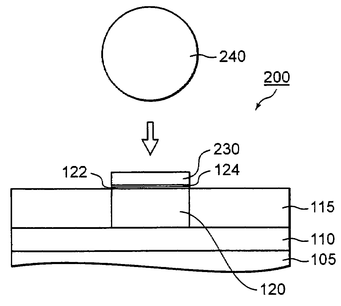
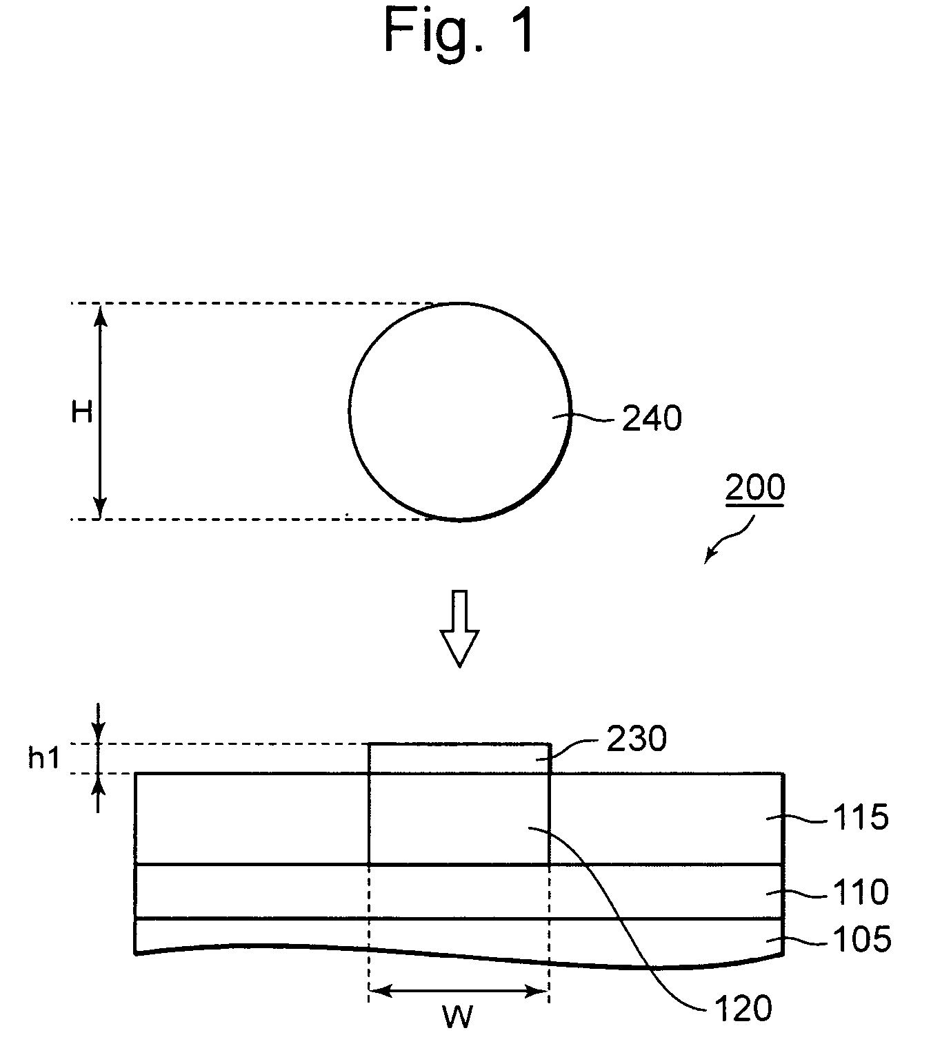
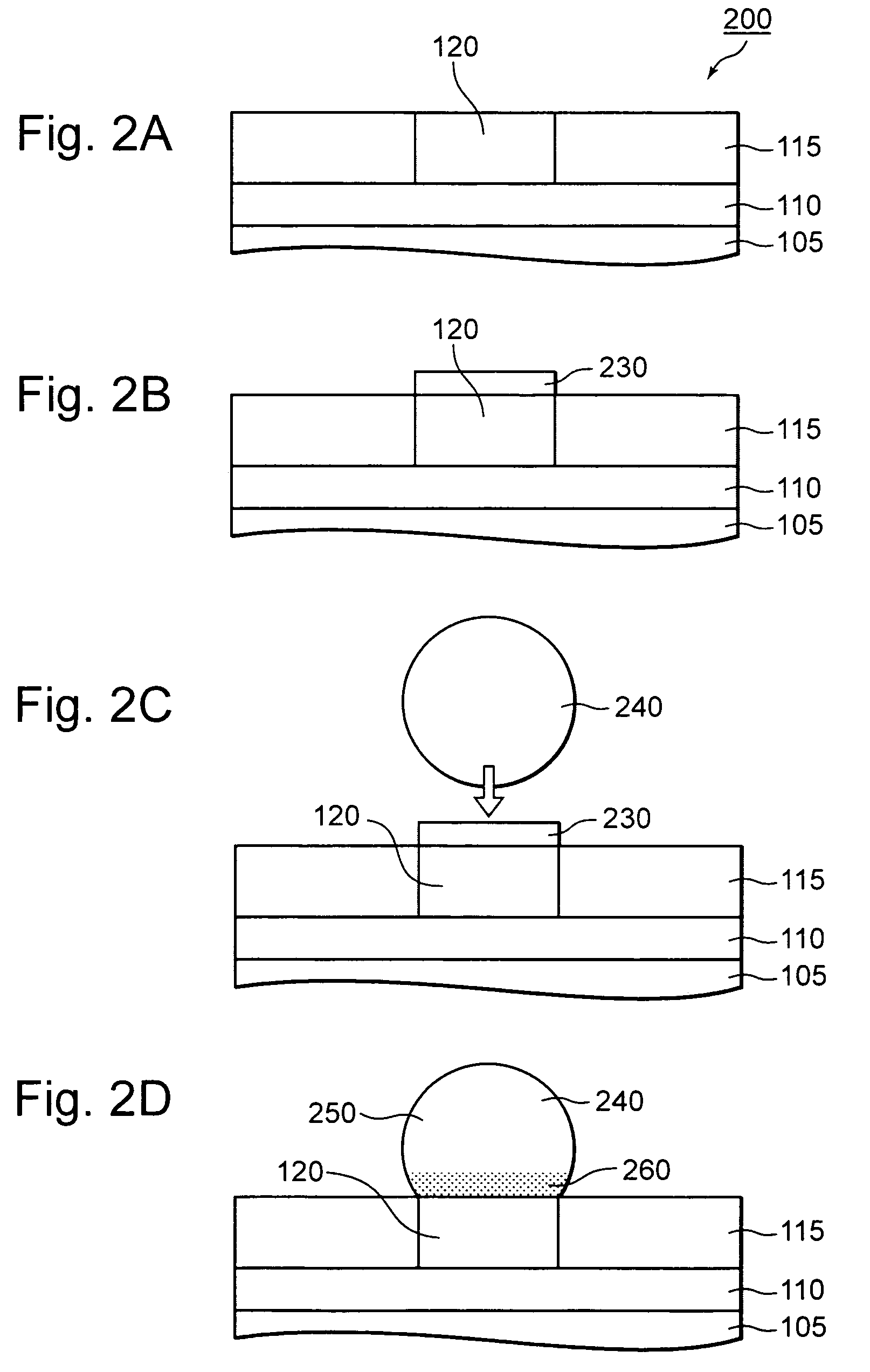
[0081]A structure of a junction (hereinafter called simply “junction structure”) between a terminal pad 120 and solder 240, according to the present invention is provided with a reactive product layer comprised of a component of the terminal pad 120 and a Zn system or based material, which is provided between the terminal pad 120 formed over an underbed or underlying base and the solder 240 (refer to FIG. 2(D), FIG. 6(B), FIG. 8(D) and FIG. 9(B)).

[0082]The junction structure of the present invention can be applied to a spot where the terminal pad and the solder are both provided in a semiconductor device. The junction structure of the present invention can be applied even to spots where the terminal pad is provided at a substrate and the solder is provided in the semiconductor device.

[0083]The junction structure according to the first embodiment will be described below in detail with the semiconductor device having the junction structure as an example. Incidentally, the first embodi...

second preferred embodiment

[0139]A junction structure according to a second embodiment will be described below in detail with a semiconductor device having this junction structure as an example. Incidentally, the second embodiment is configured such that a Zn system material (Zn in the present embodiment) is disposed on a terminal pad by plating.

Configuration of Semiconductor Device

[0140]The configuration of the semiconductor device (hereinafter called “semiconductor device according to the second embodiment”) having the junction structure according to the second embodiment will be explained below with reference to FIG. 7. Incidentally, as the semiconductor device, a semiconductor chip equipped with an LGA will be described here by way of example.

[0141]In the first embodiment, a semiconductor chip equipped with BGA has been described as the semiconductor device 200 by way of example. In the semiconductor device 200, the height from the solder terminal, i.e., the exposed surface of the Cu pad 120 to the tip of...


PUM


Abstract

A junction structure, and a semiconductor device including the same, for a junction of a terminal pad and solder, including an underlying base on which said terminal pad is formed; a nickel layer disposed on the terminal pad; a palladium layer or a gold layer disposed on the nickel layer; the solder; and a zinc system material layer provided between the palladium layer or the gold layer and the solder. The terminal pad and the solder may be provided in a semiconductor device in which the terminal pad lies inside the semiconductor device, and the zinc system material layer is formed between the terminal pad and the solder. The terminal pad may be provided over a substrate, the solder may be provided in the semiconductor device, and the zinc system material layer is then formed between the terminal pad of the substrate and the solder of the semiconductor device.

Description

BACKGROUND OF THE INVENTION[0001]1. Field of the Invention[0002]The present invention relates to a structure for a junction of a terminal pad and solder, wherein the terminal pad formed on an underlying base and the solder are joined to each other satisfactorily. The present invention also relates to a semiconductor device having the junction structure, and a method for manufacturing the semiconductor device.[0003]2. Description of the Related Art[0004]A semiconductor chip equipped with solder made molten by a heating process, such as a solder BGA (Ball Grid Array), an LGA (Land Grid Array) or the like, is in widespread use as a semiconductor device.[0005]When the semiconductor device is manufactured, the solder, such as the BGA, LGA or the like, is bonded or joined to its corresponding terminal pad formed on an exposed surface of the semiconductor device (refer to, for example, Japanese Unexamined Patent Publication No. 2002-261105 (paragraphs 69 to 76 and FIG. 17). Further, when t...

Claims


Application Information

Patent Timeline
Patent Type & Authority Patents(United States)
IPC IPC(8): H01L23/48H01L23/52H01L29/40
CPCH01L23/49811H01L24/11H01L24/05H01L24/12H01L24/16H05K3/244H01L2924/0002H01L2224/11334H01L2224/13111H01L2924/01006H01L2224/0401H01L2224/05568H01L2224/1132H01L2224/13022H01L2224/13023H01L2224/13099H01L2224/16225H01L2924/01004H01L2924/01005H01L2924/01012H01L2924/01013H01L2924/01028H01L2924/01029H01L2924/0103H01L2924/01033H01L2924/01046H01L2924/01047H01L2924/0105H01L2924/01074H01L2924/01078H01L2924/01079H01L2924/01082H01L2924/01327H01L2924/014H05K3/3436H05K3/3463H01L2924/00014H01L2224/05552H01L2924/351H01L2924/00H01L23/48
Inventor TANAKA, YASUO
Owner LAPIS SEMICON CO LTD
Why Eureka
Try Eureka