Method of calibrating an interferometer optics and of processing an optical element having an optical surface

a technology of optical elements and interferometers, applied in the direction of instruments, geometric properties/aberration measurements, structural/machine measurement, etc., can solve the problem of limited correspondence between lateral coordinate positions on the optical surface and the camera determined by the conventional method, and achieve the effect of achieving a higher degree of accuracy

Inactive Publication Date: 2008-10-14
CARL ZEISS SMT GMBH
View PDF19 Cites 22 Cited by
  • Summary
  • Abstract
  • Description
  • Claims
  • Application Information

AI Technical Summary

Benefits of technology

[0010]The present invention was made in view of the aforementioned problems, and it is an object of the present invention to provide a method for calibrating an interferometer apparatus allowing to determine optical properties of an interferometer optics with a higher degree of accuracy.
[0011]A further object of the present invention is to provide a method of qualifying and manufacturing an optical element using an interferometer apparatus calibrated to a higher degree of accuracy.
[0017]It can be advantageous to form the projections and / or indentations using a same machine tool which is used for machining the optical element to be manufactured and qualified using the calibrated interferometer apparatus.

Problems solved by technology

It has been noted that the correspondence between lateral coordinate positions on the optical surface and on the camera determined by the conventional method is limited.

Method used


Image

  • Method of calibrating an interferometer optics and of processing an optical element having an optical surface
  • Method of calibrating an interferometer optics and of processing an optical element having an optical surface
  • Method of calibrating an interferometer optics and of processing an optical element having an optical surface

Examples


Embodiment Construction

[0035]Exemplary embodiments discussed below involve, among other things, interferometrically taking measurements of wavefronts generated by reflecting an incident beam provided by an interferometer apparatus from surfaces to be measured. Plural conventional interferometric methods may be used for taking such measurements. Examples of such conventional interferometric methods are disclosed for example, in U.S. Pat. No. 5,361,312, U.S. Pat. No. 5,982,490 and US 2002 / 0063867A1. The full disclosure of these patents and publications are incorporated herein by reference.

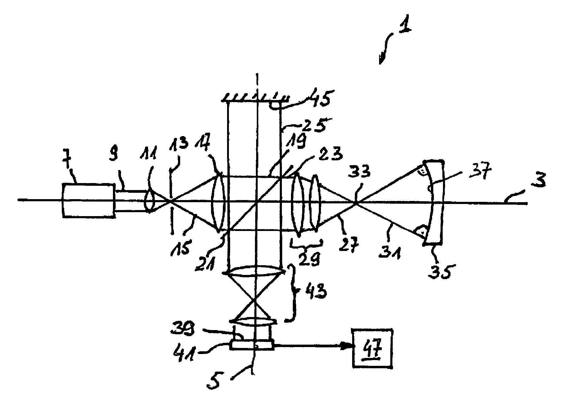
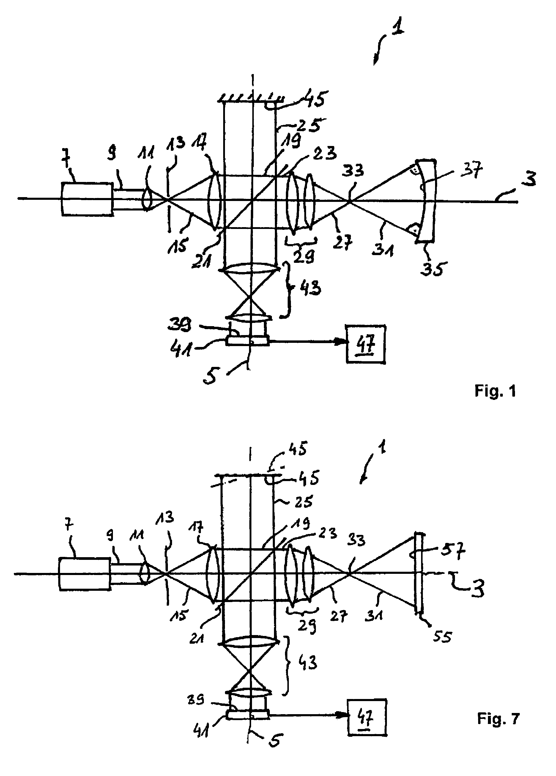
[0036]FIG. 1 illustrates an interferometer apparatus 1 used for measuring and qualifying optical elements to be manufactured. The interferometer apparatus 1 is of a Twyman-Green type having an optical axis 3 intersecting a transverse optical axis 5. A laser light source 7 such as a helium neon gas laser emits a beam 9 of measuring light having a wavelength λ 632.8 nm along optical axis 3. An objective 11 collimates light b...


PUM


Abstract

A method of calibrating an interferometer apparatus uses a calibrating element having a plurality of structures comprising at least one of projections and indentations formed on a surface of the calibrating element at predetermined positions to generate interference fringes in the interferometer apparatus to be calibrated.

Description

BACKGROUND OF THE INVENTION[0001]1. Field of the Invention[0002]The present invention relates to the field of measuring and manufacturing optical surfaces. In particular the invention relates to a method of calibrating an interferometer apparatus for measuring an optical surface and / or a method of processing the optical surface by using the interferometer apparatus.[0003]2. Brief Description of Related Art[0004]An optical substrate having the optical surface can be, for example, an optical component such as an optical lens or an optical mirror used in optical systems, such as telescopes used in astronomy, or systems used for imaging structures, such as structures of a mask or reticle onto a radiation sensitive substrate, such as a resist in a lithographic process. The success of such an optical system is substantially determined by the precision with which the optical surface can be machined or manufactured to have a target shape. In such manufacture, it is necessary to compare the ...

Claims


Application Information

Patent Timeline
Patent Type & Authority Patents(United States)
IPC IPC(8): G01B11/02
CPCG01B11/2441G01M11/025G01M11/0271G01B9/02039G01B9/02057G01B9/02072
Inventor DOERBAND, BERND
Owner CARL ZEISS SMT GMBH
Why Eureka
Try Eureka