
Fabrication of long range periodic nanostructures in transparent or semitransparent dielectrics

a technology of semi-transparent dielectrics and periodic nanostructures, applied in the field of nanotechnology, can solve problems such as grating formation, and achieve the effect of relieving build-up stress

Active Publication Date: 2008-10-21
NAT RES COUNCIL OF CANADA
View PDF3 Cites 21 Cited by
  • Summary
  • Abstract
  • Description
  • Claims
  • Application Information

AI Technical Summary

Benefits of technology

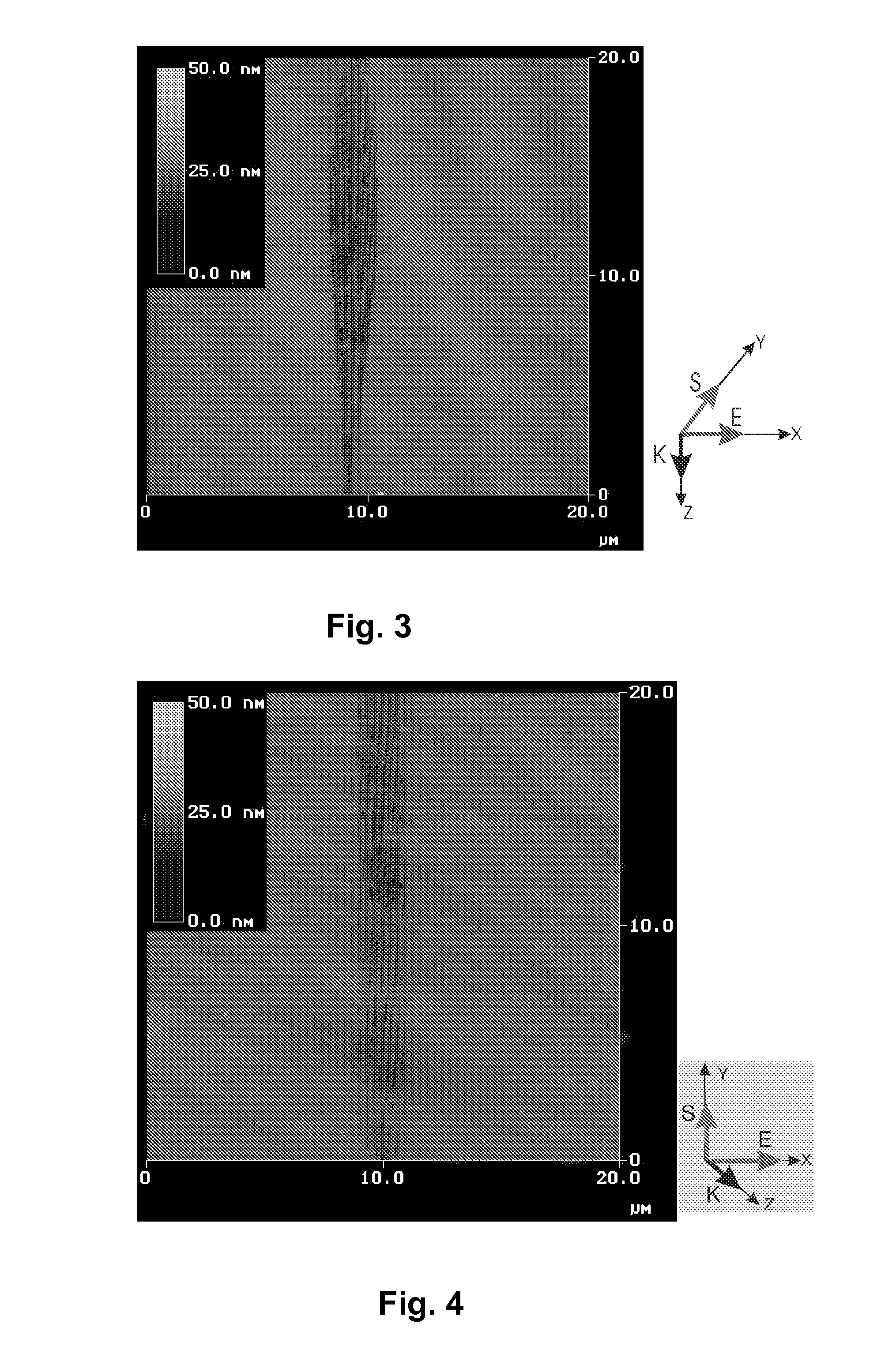
[0012]According to the present invention there is provided a method of making high quality long-range periodic nanostructures in a transparent or semi-transparent substrate, comprising generating a linearly polarized, pulsed femtosecond high repetition rate laser beam, said laser beam having an energy per pulse exceeding a predetermined energy threshold (Eth), dependent on the nature of the substrate; bringing said laser beam to a focus within the body of said transparent or semi-transparent substrate; and scanning said transparent or semi-transparent substrate with said linearly polarized laser beam along a scanning path to create sub-diffraction limit structures comprising periodic slabs of modified material oriented orthogonal to the direction of the laser polarization and extending along said scanning path in said transparent or semi-transparent substrate.
[0015]The inventors have found that one method of altering the nanoslab periodicity, which is especially important for Bragg grating applications, is to vary the laser wavelength. Periodic nanostructures have been produced with the second harmonic of the 800 nm light, i.e. at a wavelength of 400 nm. The periodicity was reduced by a factor of two approximately linearly with the wavelength and according to a λ / 2n relationship (λ wavelength; n refractive index of the dielectric) which will be discussed later. It should be possible to increase the nanoslab periodicity by using a longer wavelength laser source such as an optical parametric amplifier. This will allow the fabrication of periodic nanoslabs with spacings of interest to telecom applications.
[0020]The applicants have also made the important observation that it was possible to write a new grating in place of an existing grating. The orientation of the new grating planes was perpendicular to the new laser polarization direction. This has been accomplished for both spot (fixed focus) irradiation as well as for continuous scanning. It is believed that using a similar irradiation dosage to that used to form the original grating erases the first grating then replaces it with a second set of grating planes oriented perpendicular to the polarization direction of the rewrite beam. The ability of being able to write micron sized grating voxels inside glass in combination with a rewrite capability makes this technique attractive for 3-D data storage applications, particularity in the area of creating secure encryption codes. If the dosage of the rewrite beam is substantially lower than the write beam, it is possible to have both the write and rewrite sets of grating planes present in the material opening up the possibility of 2-D photonic crystal applications.

Problems solved by technology

Continuation of this process results in the formation of a grating.

Method used


Image

  • Fabrication of long range periodic nanostructures in transparent or semitransparent dielectrics
  • Fabrication of long range periodic nanostructures in transparent or semitransparent dielectrics
  • Fabrication of long range periodic nanostructures in transparent or semitransparent dielectrics

Examples


Embodiment Construction

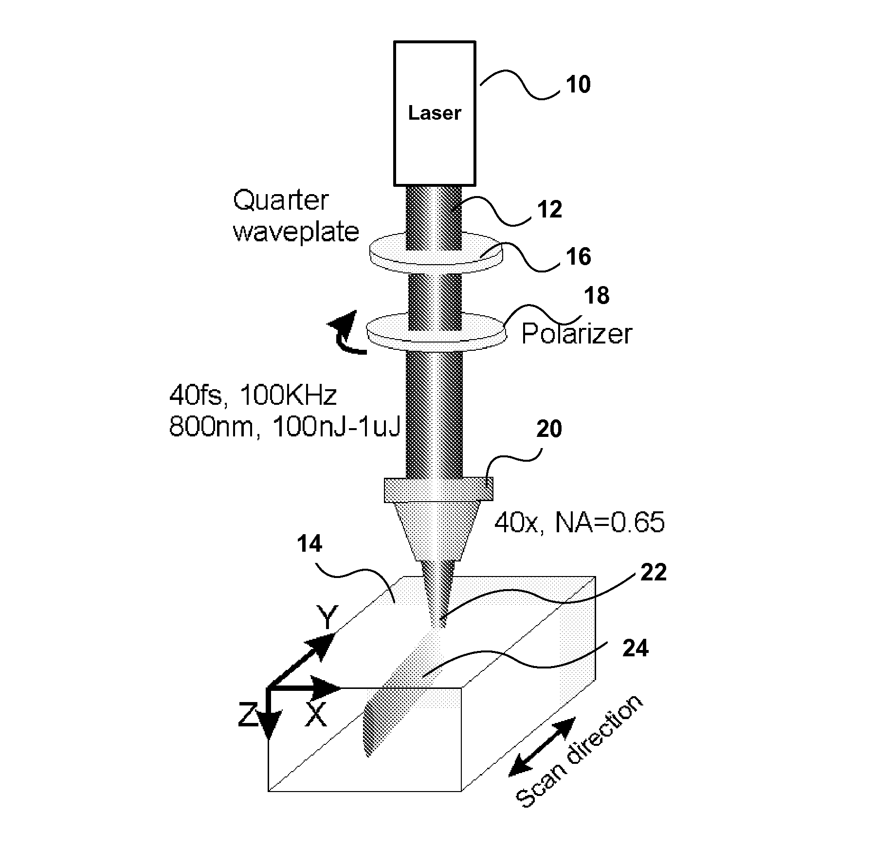
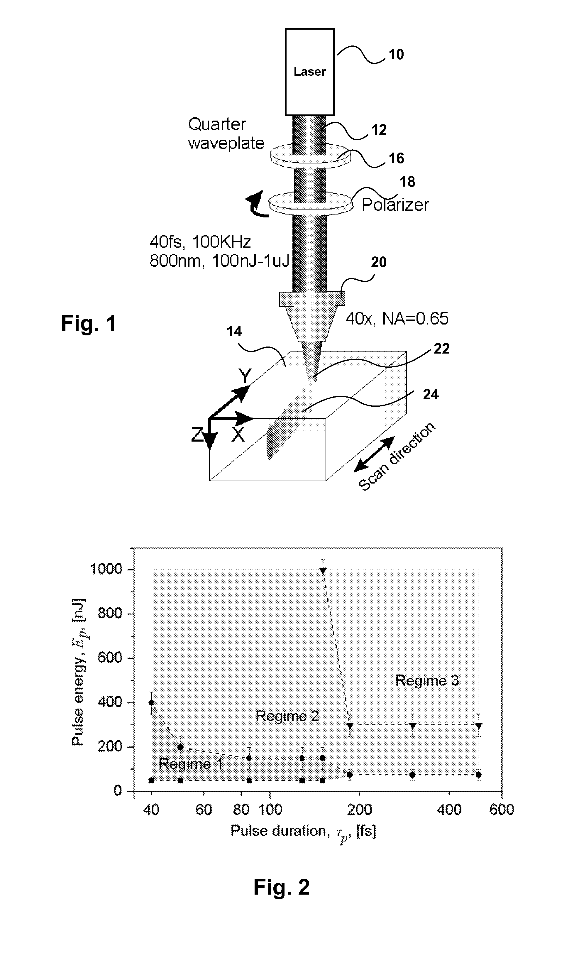
[0037]An apparatus for producing high quality long-range periodic sub-diffraction limit nanostructures using FLDM in accordance with one embodiment of the invention is shown in FIG. 1. This apparatus comprises a Ti:sapphire near-infrared femtosecond laser 10 generating laser beam 12, which is directed onto a transparent substrate 14 of fused silica. Other configurations for laser writing such as longitudinal excitation (scan direction is parallel to the light propagation direction) can also be used. It is also possible to overlap consecutive writing beams to create a wider region of grating-like slabs. As mentioned previously the degree of overlap should be approximately 50-70% of the width of the original laser written single-pass modified region. Such overlap is necessary so that the sub-wavelength periodicity of the first laser written modified region is transferred or imposed coherently onto the second laser modified region etc. so that the broader modified region has a single p...


PUM

PropertyMeasurementUnit
energyaaaaaaaaaa
temperaturesaaaaaaaaaa
lengthsaaaaaaaaaa

Abstract

To make high quality long-range periodic nanostructures in a transparent or semi-transparent substrate, the transparent or semi-transparent substrate is scanned with a linearly polarized laser beam generated by a femtosecond laser and exceeding a predetermined energy / pulse threshold along a scanning path. Sub-diffraction limit structures are formed as periodic planes of modified material in the transparent or semi-transparent substrate extending along the scanning path. The modified material can then be chemically etched to form cavities.

Description

CROSS REFERENCE TO RELATED APPLICATION[0001]This application claims the benefit under 35 USC 119(e) of U.S. provisional application no. 60 / 664,946 filed Mar. 25, 2005, the contents of which are herein incorporated by reference.FIELD OF THE INVENTION[0002]This invention relates to the field of nanotechnology, and in particular to a method of making long-range periodic nanostructures inside transparent or semi-transparent dielectrics.BACKGROUND OF THE INVENTION[0003]Periodic structures of nanometer dimensions but with long-range order (at least mms) inside transparent materials such as fused silica and other optical glasses have a variety of applications. Optical methods, such as femtosecond (1 fs=10−15 s) laser dielectric modification (FLDM), for fabricating such structures have advantages over traditional micro-fabrication techniques which for the most part only allow the fabrication on a surface and not inside the bulk material. In fact FLDM is the only viable technique capable of ...

Claims


Application Information

Patent Timeline
Patent Type & Authority Patents(United States)
IPC IPC(8): B44C1/22
CPCB23K26/0039B23K26/365B82Y20/00G02B6/02123G02B6/107G02B6/1225Y10S430/146B23K26/0006B23K26/361B23K2103/50
Inventor TAYLOR, RODCORKUM, PAULVEDULA, RAVI BHARDWAJSIMOVA, ELIRAYNER, DAVIDHNATOVSKY, CYRIL
Owner NAT RES COUNCIL OF CANADA
Learn More