Display device and method for driving the same

a technology of display device and display method, applied in the field of display device, can solve the problems of reducing the number of pixels which can be displayed accordingly, and the above-mentioned problem is more conspicuous, and achieves the effect of shortening the selection period per pixel

Active Publication Date: 2008-10-28
SHARP KK
View PDF18 Cites 35 Cited by
  • Summary
  • Abstract
  • Description
  • Claims
  • Application Information

AI Technical Summary

Benefits of technology

[0023]The present invention is designed to solve the foregoing problems and has as an object to realize a display device which makes it possible to shorten a selection period per pixel while compensating variations in a threshold voltage of a driving transistor, and a method for driving the same.
[0025]According to the foregoing invention, a potential corresponding to display data of the pixel is supplied to the current control terminal of the driving transistor before or at the same time as the first period. Moreover, by compensating a threshold voltage of the driving transistor which has been put in an ON state in the first period, the potential of the current control terminal of the driving transistor becomes larger than a potential Vs of the reference potential terminal of the driving transistor by a threshold voltage Vth. Further, although a threshold voltage of the driving transistor which has been put in an OFF state cannot be compensated, there is no problem, because an OFF state is not dependent on a threshold voltage. Moreover, by changing, in the second period, the potential of the current control terminal of the driving transistor or the potential of the reference potential terminal of the driving transistor, an output current of the driving transistor can be set a desired current value regardless of a threshold voltage.
[0027]According to the foregoing invention, before the first period, the second switching transistor is put in an ON state and the first switching transistor is also put in an ON state, so that the driving transistor can be put in an ON state. Moreover, by compensating a threshold voltage of the driving transistor which has been put in an ON state in the first period, the potential of the current control terminal of the driving transistor becomes larger than a potential Vs of the reference potential terminal of the driving transistor by a threshold voltage Vth. Moreover, a potential corresponding to display data of the pixel is supplied from the data wire to the current control terminal of the driving transistor, so that a potential of the other terminal of the first capacitor or a potential of the reference potential terminal of the driving transistor is changed. In this way, an output current of the driving transistor can be set at a desired current value regardless of a threshold voltage.
[0028]The data wire only needs to be connected to the pixel at least from the time that a potential corresponding to display data of the pixel is supplied to the current control terminal of the driving transistor until a corresponding charge is stored the first capacitor. Therefore, the pixel does not need to occupy the data wire in a period during which a threshold voltage of the driving transistor is compensated. This brings about an effect of achieving a display device which makes it possible to shorten a selection period per pixel while compensating variations in the threshold voltage of the driving transistor.

Problems solved by technology

However, the foregoing problem occurs more conspicuously.
This raises a problem that the number of pixels which can be displayed decreases accordingly.

Method used


Image

  • Display device and method for driving the same
  • Display device and method for driving the same
  • Display device and method for driving the same

Examples


first embodiment

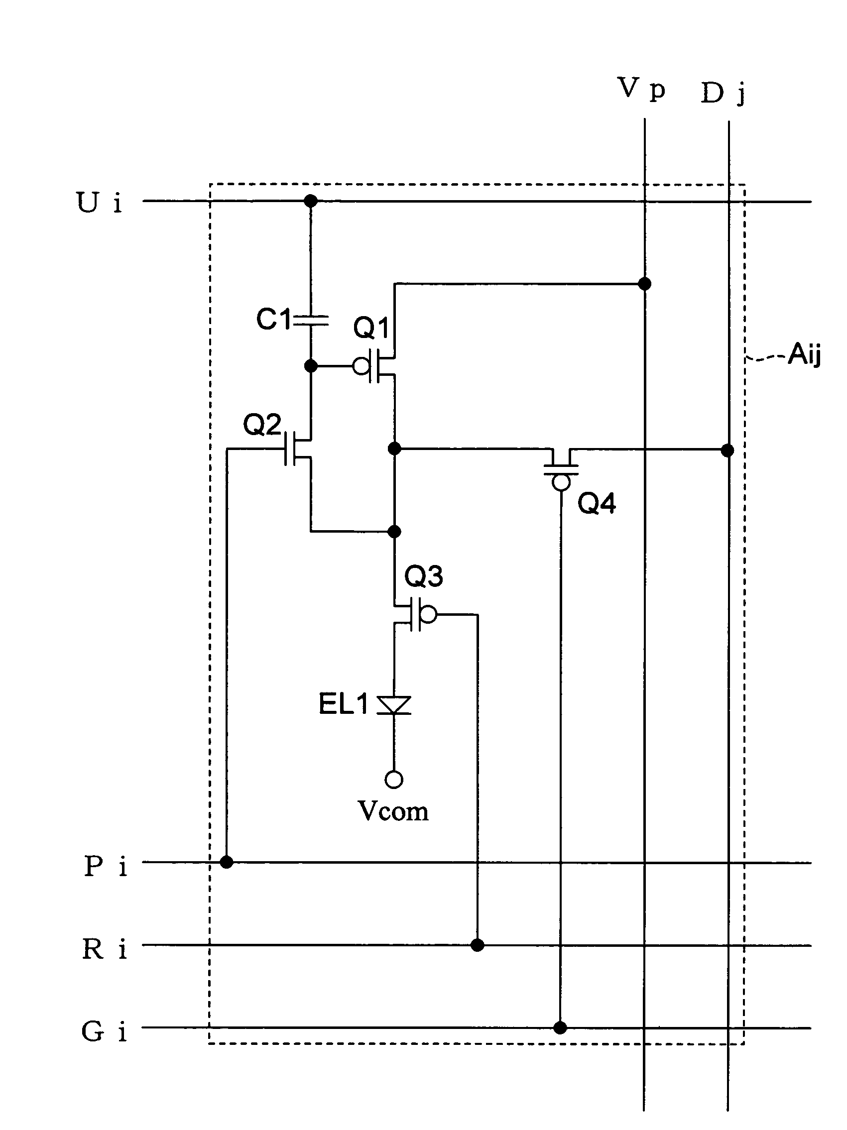
[0060]In the present embodiment, a first example of a display device of the present invention will be described.

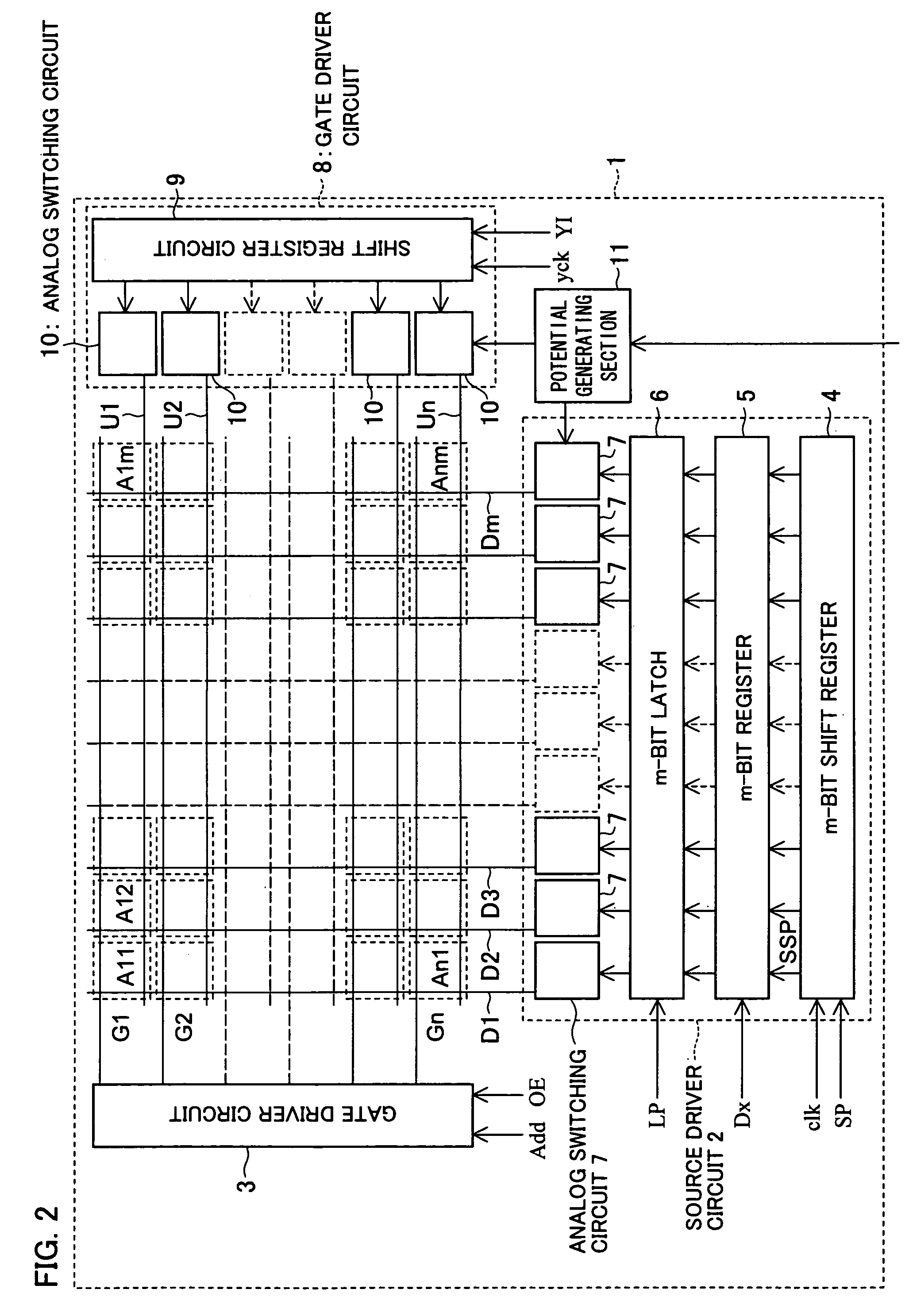
[0061]A display device 1 of the present embodiment, as shown in FIG. 2, has pixel circuits Aij (i=1 to n, j=1 to m), gate drivers 3 and 8, a source driver 2, and a potential generating section 11. The pixel circuits Aij are disposed in a matrix manner. The gate drivers 3 and 8 and a source driver circuit 2 serve as a wiring control circuit for the pixel circuits Aij. The potential generating section 11 serves as an internal voltage generating circuit.

[0062]Each of the pixel circuits Aij is disposed in a region where a data wire Dj and a gate wire Gi intersect with each other. Further, the source driver circuit 2 includes an m-bit shift register 4, an m-bit register 5, an m-bit latch 6, and m-number of analog switch circuits 7.

[0063]In the source driver circuit 2, a first register of the m-bit shift register 4 receives a start pulse SP, and the start pulse SP is transferred...

second embodiment

[0116]In the present embodiment, a second example of the display device according to the present invention will be described.

[0117]Since a display device 1 according to the present embodiment also has the same arrangement as shown in FIG. 2, the description is omitted.

[0118]FIG. 11 shows an arrangement of a pixel circuit Aij according to the present embodiment.

[0119]The pixel circuit Aij has an n-type switching TFT: Q5 (fourth switching transistor) disposed between a gate terminal (current control terminal) of a driving TFT: Q1 (driving transistor) and a data wire Dj instead of the switching TFT: Q4 (third switching transistor) of the pixel circuit Aij of FIG. 1. Since the pixel circuit of FIG. 11 is the same as the pixel circuit of FIG. 1 otherwise, a further description thereof is omitted here.

[0120]Operation of the pixel circuit Aij will be described below with reference to a timing chart of FIG. 12.

[0121]In FIG. 12, Ui, G1, Ri, and Pi correspond to the pixel circuit Aij, and Ui+...

third embodiment

[0143]In the present embodiment, a third example of the display device according to the present invention will be described.

[0144]Since a display device 1 according to the present embodiment also has the same arrangement as shown in FIG. 2, the description thereof is omitted.

[0145]FIG. 15 shows an arrangement of a pixel circuit Aij according to the present embodiment.

[0146]The pixel circuit Aij has a capacitor C3 (second capacitor) provided between a drain terminal (current output terminal) of a driving TFT: Q1 (driving transistor) and a data wire Dj instead of the switching TFT: Q4 (third switching transistor) of the pixel circuit Aij of FIG. 1. Further, the gate wire Gi for controlling a gate voltage of the switching TFT: Q4 is also removed. Since the pixel circuit of FIG. 15 is the same as the pixel circuit of FIG. 1 otherwise, a further description thereof is omitted here.

[0147]Operation of the pixel circuit Aij will be described below with reference to a timing chart of FIG. 16...


PUM


Abstract

A display device which makes it possible to shorten a selection period per pixel while compensating variations in a threshold voltage of the driving transistor, and a method for driving the same are achieved. In a pixel circuit Aij, a potential wire Ui is set to a potential Vcc, a voltage of a gate wire Gi becomes Low, a voltage of a control wire Ri becomes High, and a voltage of a control wire Pi becomes High, so that a gate terminal of a driving TFT: Q1 has a potential of a data wire Dj. Moreover, a voltage of the gate wire Gi becomes High so as to compensate a threshold voltage of the driving TFT: Q1. Thereafter, a voltage of the control wire Pi becomes Low, and the potential wire Ui is set to a potential Vc, so that a voltage of a capacitor C1, i.e., a gate-source voltage of the driving TFT is changed. This causes a voltage of the control wire Ri to be Low, so that a driving current is flown into an organic EL: EL1.

Description

[0001]This Nonprovisional application claims priority under 35 U.S.C. § 119(a) on Patent Application No. 2004 / 254615 filed in Japan on Sep. 1, 2004, the entire contents of which are hereby incorporated by reference.FIELD OF THE INVENTION[0002]The present invention relates to a display device using a current-driven electro-optic element such as an organic EL (electroluminescence) display or an FED (field emission display). The present invention also relates to a method for driving the display device.BACKGROUND OF THE INVENTION[0003]Recently, research and development of a current-driven light-emitting element such as an organic EL (electroluminescence) display or an FED have been actively carried out. Particularly, an organic EL display is a display which can emit light at low voltage and with low power consumption, and draws attention as being used for a mobile device such as a mobile phone or a PDA (personal digital assistance).[0004]As an arrangement of a current-driven pixel circu...

Claims


Application Information

Patent Timeline
Patent Type & Authority Patents(United States)
IPC IPC(8): G09G3/30
CPCG09G3/3233G09G2300/0819G09G2300/0842G09G2300/0852G09G2300/0861G09G2300/0866G09G2300/0876G09G2320/043
Inventor NUMAO, TAKAJI
Owner SHARP KK
Why Eureka
Try Eureka