Memory array bit line coupling capacitor cancellation

a memory array and capacitor technology, applied in the field of memory array bit line coupling capacitor cancellation, can solve the problems of inability to cancel memory arrays, and inability to read data in certain conditions

Active Publication Date: 2008-10-28
INTEGRATED DEVICE TECH INC
View PDF3 Cites 7 Cited by
  • Summary
  • Abstract
  • Description
  • Claims
  • Application Information

AI Technical Summary

Problems solved by technology

The parasitic capacitances CA, CB and CAB can result in erroneous read operations in certain conditions.
As a result, the voltage on bit line BLB is undesirably reduced.
However, the formation of a metal line for each column of the memory array disadvantageously requires a relatively large layout area.
However, electrical coupling still exists between bit lines BLA and BLB, which can result in the erroneous read conditions described above.

Method used


Image

  • Memory array bit line coupling capacitor cancellation
  • Memory array bit line coupling capacitor cancellation
  • Memory array bit line coupling capacitor cancellation

Examples


Embodiment Construction

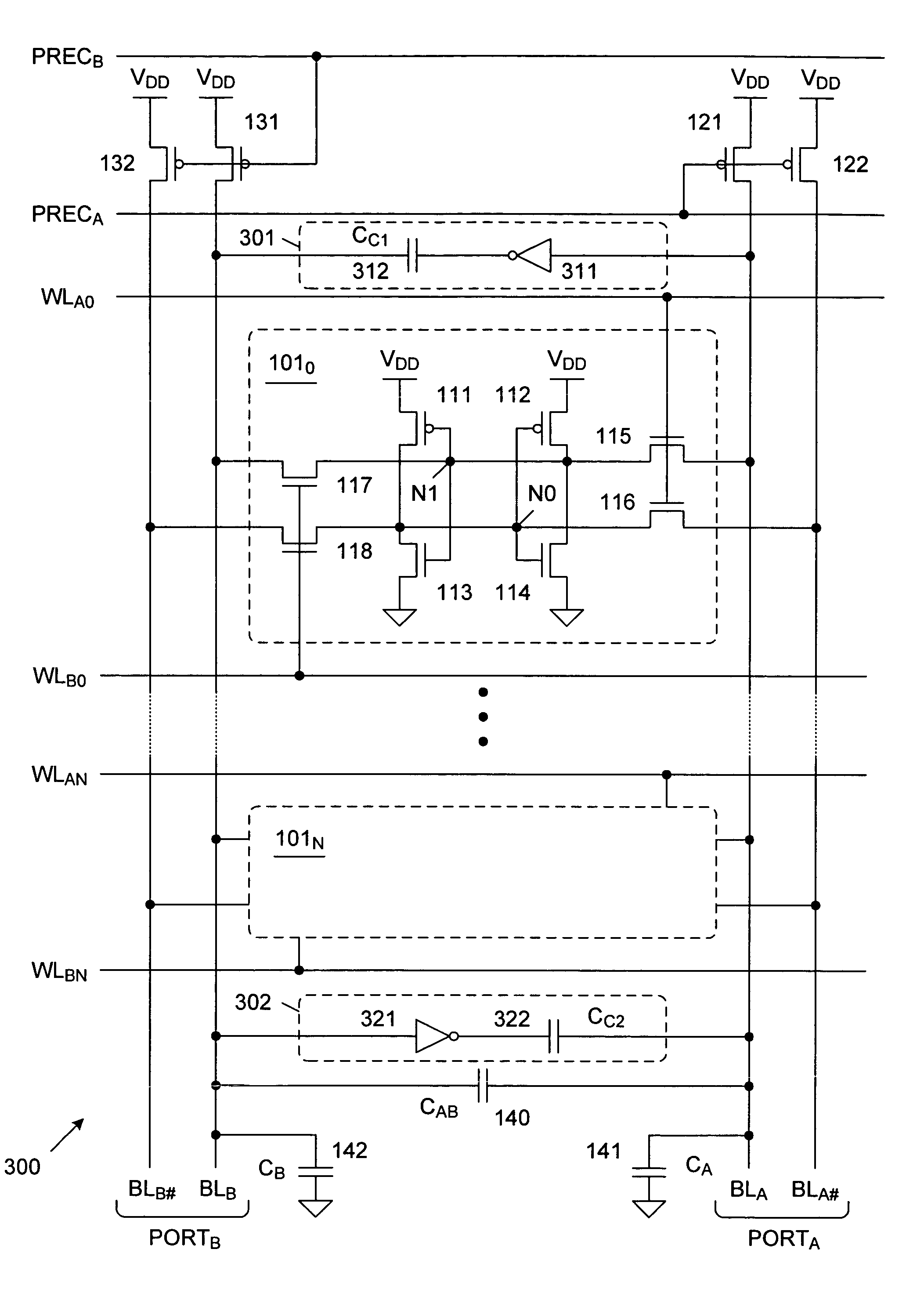
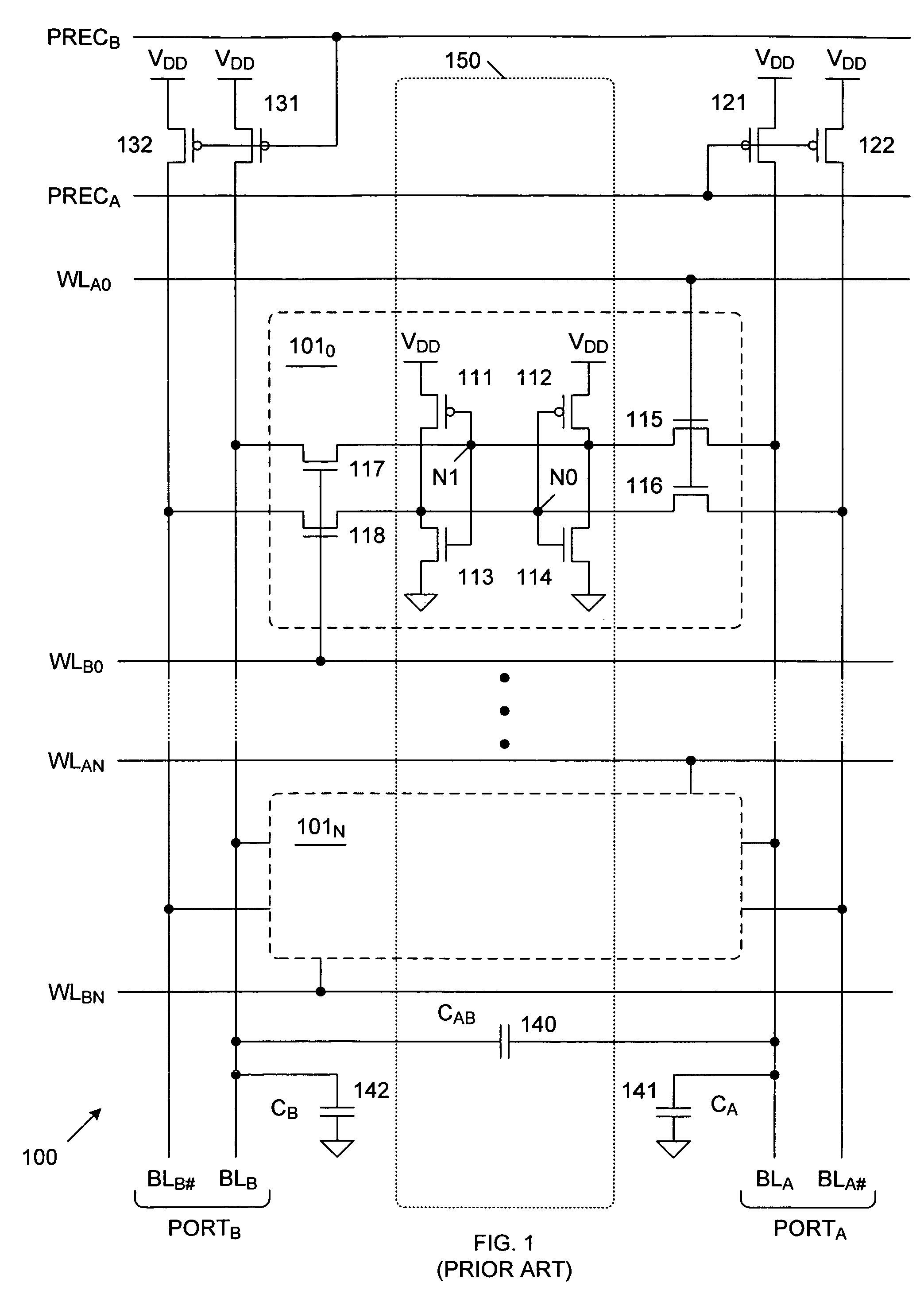
[0018]FIG. 3 is a circuit diagram of a column 300 of multi-port SRAM memory cells in accordance with one embodiment of the present invention. It is understood that any number of SRAM columns, identical to SRAM column 300, can be combined to form a memory array. Similar elements in FIGS. 1 and 3 are labeled with similar reference numbers. Thus, SRAM column 300 includes dual-port SRAM memory cells 1010–101N, p-channel pre-charge transistors 121–122 and 131–132, pre-charge lines PRECA and PRECB, word lines WLA0–WLAN and WLB0–WLBN, bit lines BLA–BLA# and BLB–BLB#, and parasitic capacitance elements 140-142, which have been described above in connection with FIG. 1.

[0019]In addition, SRAM column 300 includes capacitive coupling correction circuits 301 and 302. Capacitive coupling correction circuit 301 includes inverter 311 and capacitor 312. Inverter 311 has an input terminal coupled to bit line BLA and an output terminal coupled to capacitor 312. Capacitor 312 is further coupled to bit...


PUM


Abstract

Capacitive coupling correction circuits are coupled between adjacent parallel dynamic (pre-charged) or static conductors. The capacitive coupling correction circuits effectively isolate a low voltage applied to a first conductor from a high pre-charged voltage stored on an adjacent second conductor (or vice versa). The adjacent parallel conductors can be bit lines of a memory cell. Each capacitive coupling correction circuit can include an inverter having an input terminal coupled to the first conductor, and an output terminal coupled to a first plate of a capacitor. A second plate of the capacitor is coupled to the second conductor. The capacitance of the capacitor is selected to be identical to a parasitic capacitance between the first and second conductors. As a result, there is a zero net voltage effect between the first and second conductors. The capacitive coupling correction circuits may be distributed along the length of the first and second conductors.

Description

RELATED APPLICATION[0001]The present application is related to and claims priority of U.S. Provisional Patent Application Ser. No. 60 / 600,351 filed by Chuen-Der Lien and Tzong-Kwang Henry Yeh on Aug. 9, 2004.FIELD OF THE INVENTION[0002]The present invention relates to systems that implement parallel dynamic (pre-charged) nodes and parallel static nodes.RELATED ART[0003]FIG. 1 is a circuit diagram of a column 100 of a conventional dual-port static random access memory (SRAM) array. SRAM column 100 includes dual-port SRAM memory cells 1010–101N, p-channel pre-charge transistors 121–122 and 131–132, pre-charge enable lines PRECA and PRECB, word lines WLA0–WLAN and WLB0–WLBN and bit lines BLA–BLA# and BLB–BLB#. Bit lines BLA–BLA# are coupled to a first port (PORTA) of each memory cell of column 100, and bit lines BLB–BLB# are coupled to a second port (PORTB) of each memory cell in column 100.[0004]Dual-port SRAM cell 1010 includes p-channel pull-up transistors 111–112, n-channel pull-do...

Claims


Application Information

Patent Timeline
Patent Type & Authority Patents(United States)
IPC IPC(8): G11C7/00
CPCG11C5/063G11C7/02G11C7/12G11C8/16G11C11/419
Inventor LIEN, CHUEN-DERYEH, TZONG-KWANG HENRY
Owner INTEGRATED DEVICE TECH INC
Why Eureka
Try Eureka