System and method for circuit noise analysis

a circuit noise and noise analysis technology, applied in the direction of error detection/correction, cad circuit design, instruments, etc., can solve the problems of reducing the signal-to-noise ratio of these circuits, reducing the size of these integrated circuits, and increasing the noise resistance of these circuits, so as to achieve more sound analysis of a circuit

Active Publication Date: 2008-10-28
TOSHIBA ELECTRONICS DEVICES & STORAGE CORPORARTION +2
View PDF2 Cites 4 Cited by
  • Summary
  • Abstract
  • Description
  • Claims
  • Application Information

AI Technical Summary

Benefits of technology

[0020]Embodiments of the present invention may provide the technical advantage of a noise analysis of a circuit which can detect failures within a block of logic which may be caused by noise originating outside of the block of logic. This ability may result in a more sound analysis of a circuit or circuit design and the ability to design and implement high performance circuits without use of additional logic intended to compensate for certain types of noise.

Problems solved by technology

As the size of these integrated circuits has shrunk they have commensurately become increasingly sensitive to noise.
All of these factors degrade the signal-to-noise ratio in these circuits.
Noise has two deleterious effects on digital circuits and designs, including microprocessor designs.
Firstly, when noise acts against a normally static signal, it can transiently destroy the logical information carried by a static node in the circuit.
If this ultimately results in incorrect machine states stored in one or more latches, functional failures may result.
Secondly, when noise acts simultaneously with a switching node, this may be manifest as a change in the timing of the transition of the node, or other nodes.
As the clock speeds of these integrated circuits have increased, however, these buffers were rendered obsolete, as they introduced an unacceptable amount of delay into these high speed circuits.
If buffers are utilized in this type of circuit to reduce noise, achieving this design goal may be difficult.
However, for system-level noise simulation for a complex integrated circuit, the direct method and the adjoint method are usually too inefficient to be practically utilized.
Utilizing this technique, noise failures inside these logic blocks can only be detected at transistor level noise analysis, while noise failures at the unit / chip level can only be found at unit / chip level noise analysis.
In many cases, however, noise originating outside a block may be fed back to the block through an output of the block.
This noise feedback through an output may result in a noise failure at a gate inside a block.
For example, if a circuit topology is such that an output signal of a block also propagates to other logic inside the same block, a sufficiently large noise generated outside the block could be fed back through this output and could further proceed back through gates or logic in the block, resulting in a noise failure at a gate inside the block.

Method used


Image

  • System and method for circuit noise analysis
  • System and method for circuit noise analysis
  • System and method for circuit noise analysis

Examples


Embodiment Construction

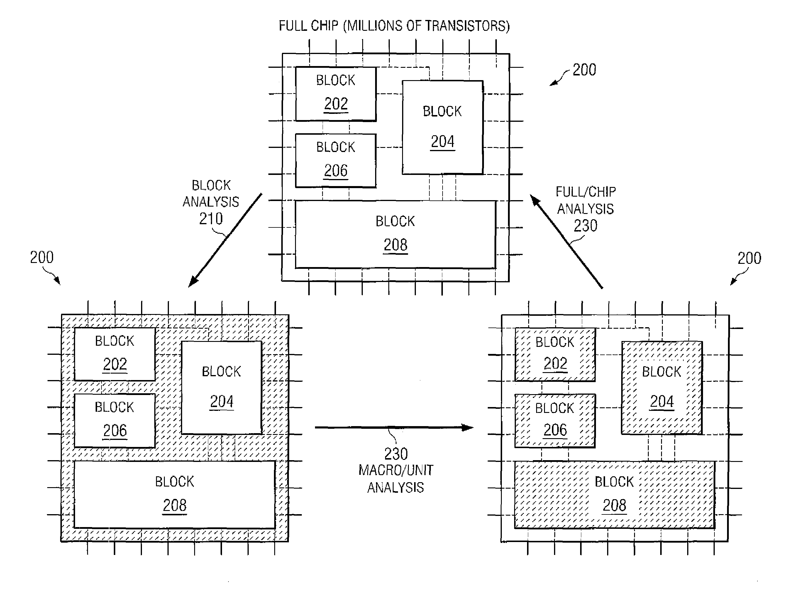
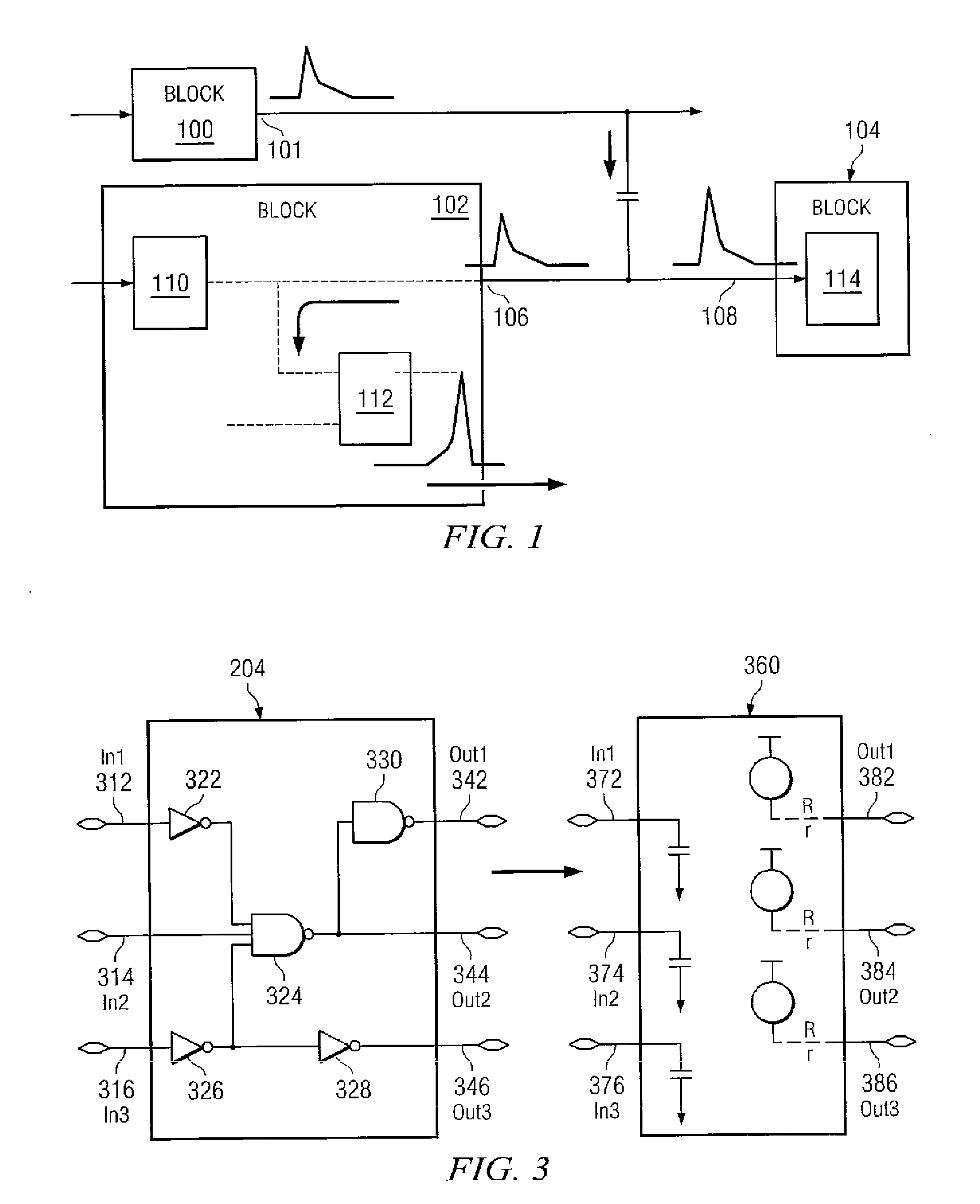
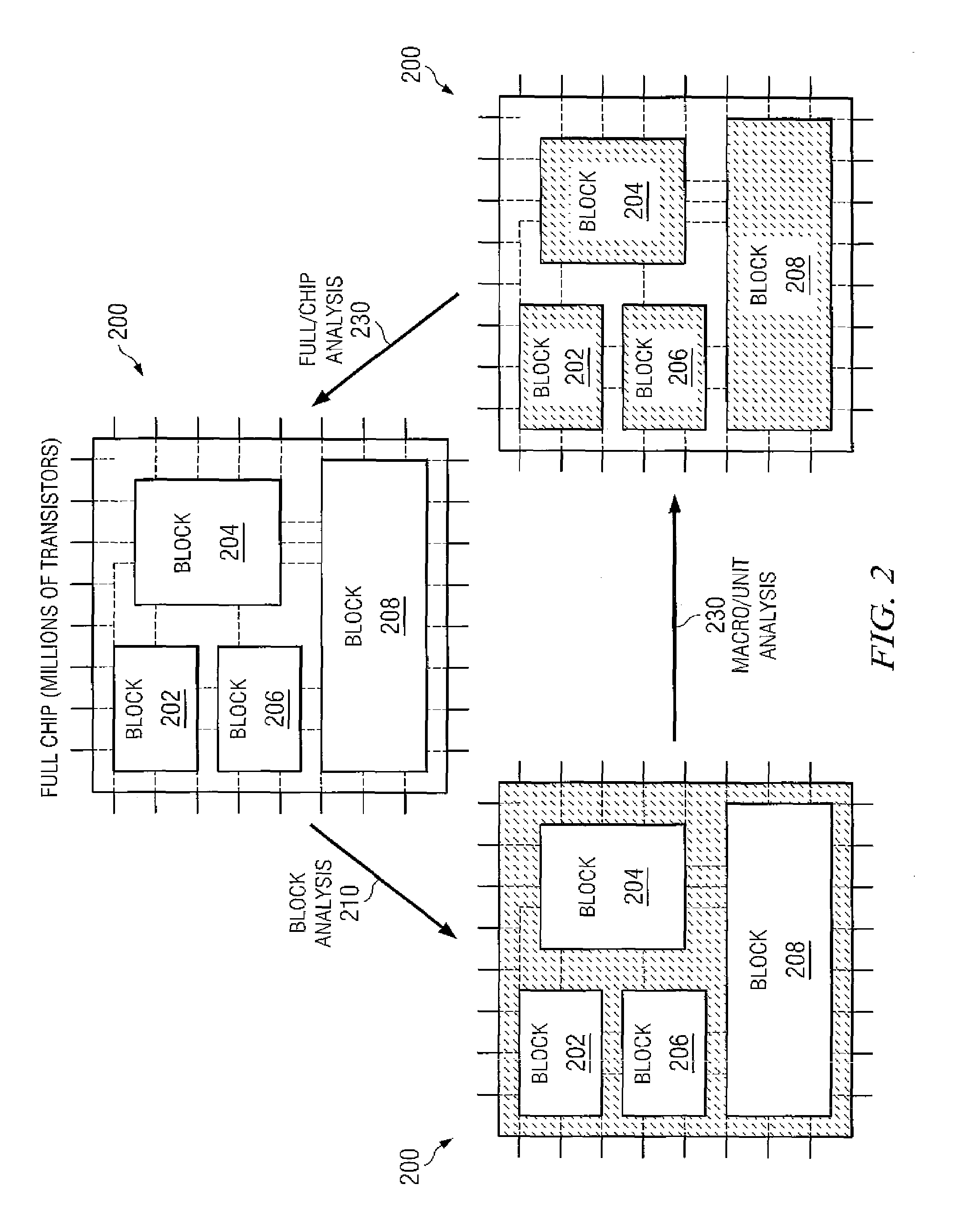
[0029]The invention and the various features and advantageous details thereof are explained more fully with reference to the nonlimiting embodiments that are illustrated in the accompanying drawings and detailed in the following description. Descriptions of well known starting materials, processing techniques, components and equipment are omitted so as not to unnecessarily obscure the invention in detail. It should be understood, however, that the detailed description and the specific examples, while indicating preferred embodiments of the invention, are given by way of illustration only and not by way of limitation. After reading the specification, various substitutions, modifications, additions and rearrangements will become apparent to those skilled in the art from this disclosure which do not depart from the scope of the appended claims.

[0030]Before describing embodiments of the system and methods of the present invention it may be useful to describe a potential cause of failure...


PUM


Abstract

Systems and methods for the noise analysis of circuits are presented. These systems and methods may allow a circuit or circuit design to be analyzed for possible noise failures in a block of logic caused by sources. outside the block. More particularly, these systems and methods may generate an abstract file for one or more blocks of a circuit. These abstract files may include noise tolerances for input pins and bi-directional pins of a block, along with noise tolerances for those output pins of the block which also feed to an input of one or more gates internal to the block. Using these noise abstracts a unit of the circuit may be analyzed, or the circuit itself may be analyzed for possible noise induced failures.

Description

TECHNICAL FIELD OF THE INVENTION[0001]The present invention relates generally to noise analysis of circuits and methods for noise analysis in circuits, and more particularly, to hierarchical noise analysis techniques.BACKGROUND OF THE INVENTION[0002]In recent years, the size of integrated circuits has decreased dramatically. As the size of these integrated circuits has shrunk they have commensurately become increasingly sensitive to noise. Integrated circuits have become more sensitive to noise for a whole host of reasons including: increasing interconnect densities within integrated circuits, faster clock rates utilized in conjunction with these integrated circuits and scaling threshold voltages. All of these factors degrade the signal-to-noise ratio in these circuits. Particularly, increasing interconnect densities imply a significant increase in coupling capacitance. Faster clock rates imply faster on-chip slew times. These two effects combine to make capacitive coupling a growin...

Claims


Application Information

Patent Timeline
Patent Type & Authority Patents(United States)
IPC IPC(8): G06F17/50
CPCG06F17/5022G06F30/33
Inventor KAMEYAMA, ATSUSHIKONANKI, SUNILSITKO, MICHAEL HENRY
Owner TOSHIBA ELECTRONICS DEVICES & STORAGE CORPORARTION
Why Eureka
Try Eureka