Plasma processing apparatus

a processing apparatus and plasma technology, applied in the direction of electric/magnetic/electromagnetic heating, coating, electric discharge lamps, etc., can solve the problems of difficult to transmit a stable microwave, high equipment and maintenance costs, etc., and achieve the effect of effective emitted

Active Publication Date: 2008-11-04
COMMSCOPE TECH LLC +1
View PDF13 Cites 17 Cited by
  • Summary
  • Abstract
  • Description
  • Claims
  • Application Information

AI Technical Summary

Benefits of technology

[0019]In accordance with the present invention, since the microwaves are transmitted to respective antennas included in the antenna section, it is not necessary to combine high power microwaves in the transmission line leading to the antenna section. Thus, a combiner is not needed to thereby be able to completely avoid the power loss due to the combiner. Further, since it is possible to lower the powers of microwaves transmitted to respective antennas, there is no need to use an isolator for a high power. Accordingly, the microwave oscillator need not be large-sized. Further, since microwaves having different powers from each other can be supplied to a plurality of antennas included in the antenna section, it becomes possible to control the output distribution of the microwave emitted from the antenna.
[0021]In this case, if each of the plurality of amplifier sections has a variable attenuator for attenuating a microwave outputted from the divider to a predetermined level; a solid state amplifier for amplifying a microwave outputted from the variable attenuator to a specified power; an isolator for separating a reflected microwave returning to the solid state amplifier from a microwave which is outputted from the solid state amplifier to the antenna; and a matcher for regulating a power of the reflected microwave, microwaves of different powers can be supplied to respective antennas by regulating an attenuation rate in each variable attenuator. Accordingly, it is possible to control the distribution of a plasma generated in the chamber.
[0023]In this case, the power of the microwave outputted from a single solid state amplifier is not extremely large such that it is possible to use a small-sized isolator to thereby cut down on manufacturing costs of the apparatus.
[0025]Since a power of a low power microwave is amplified by a semiconductor amplifying device without using a magnetron, the amplifier section can be semipermanent. Consequently, equipment costs and maintenance costs can be cut down. Further, the semiconductor amplifying device has an excellent output stability and therefore a stable microwave can be emitted into the chamber. Thus, a plasma is generated in a satisfactory condition, thereby improving quality in processing the substrate. Furthermore, in this case, a range of output control for the amplifier section is wide (0 to 100%) and the control becomes easy.
[0027]In this case, it is preferable that the circular antenna is provided with first slots of a predetermined length disposed along a circle located inwardly by λg / 4 from the periphery of the circular antenna and second slots of a specified length disposed on one or more concentric circles located inwardly at intervals of λg / 2 from the first slots. Further, it is preferable that each of the plural approximately fan-shaped antennas is provided with third slots of a preset length located inwardly by λg / 4 from respective boundaries between the approximately fan-shaped antennas and fourth slots of a specific length located inwardly at intervals of λg / 2 from the third slots. Thus, the microwave can be effectively emitted into the chamber.

Problems solved by technology

However, the microwave oscillator 91 using the magnetron 91a has a drawback such as the high cost for the equipment and the maintenance thereof due to a short life of about half a year of the magnetron 91a.
Further, since the magnetron 91a has oscillation stability of approximately 1% and output stability of approximately 3%, resulting in a large difference therebetween, it is difficult to transmit a stable microwave.
In case of impedance mismatching, power loss can be increased.
Further, in order to transmit the large power microwave outputted from the combiner 84 to the isolator 85, the isolator 85 needs to be large-sized in a few KW range, resulting in restricting the place where the isolator 85 is to be installed and further resulting in a high cost for the isolator 85 itself.
Furthermore, since the combined microwave is transmitted to the antenna 87 through a single coaxial tube, it is not possible to control the distribution of the microwave outputted from the antenna 87.

Method used


Image

  • Plasma processing apparatus
  • Plasma processing apparatus
  • Plasma processing apparatus

Examples


Embodiment Construction

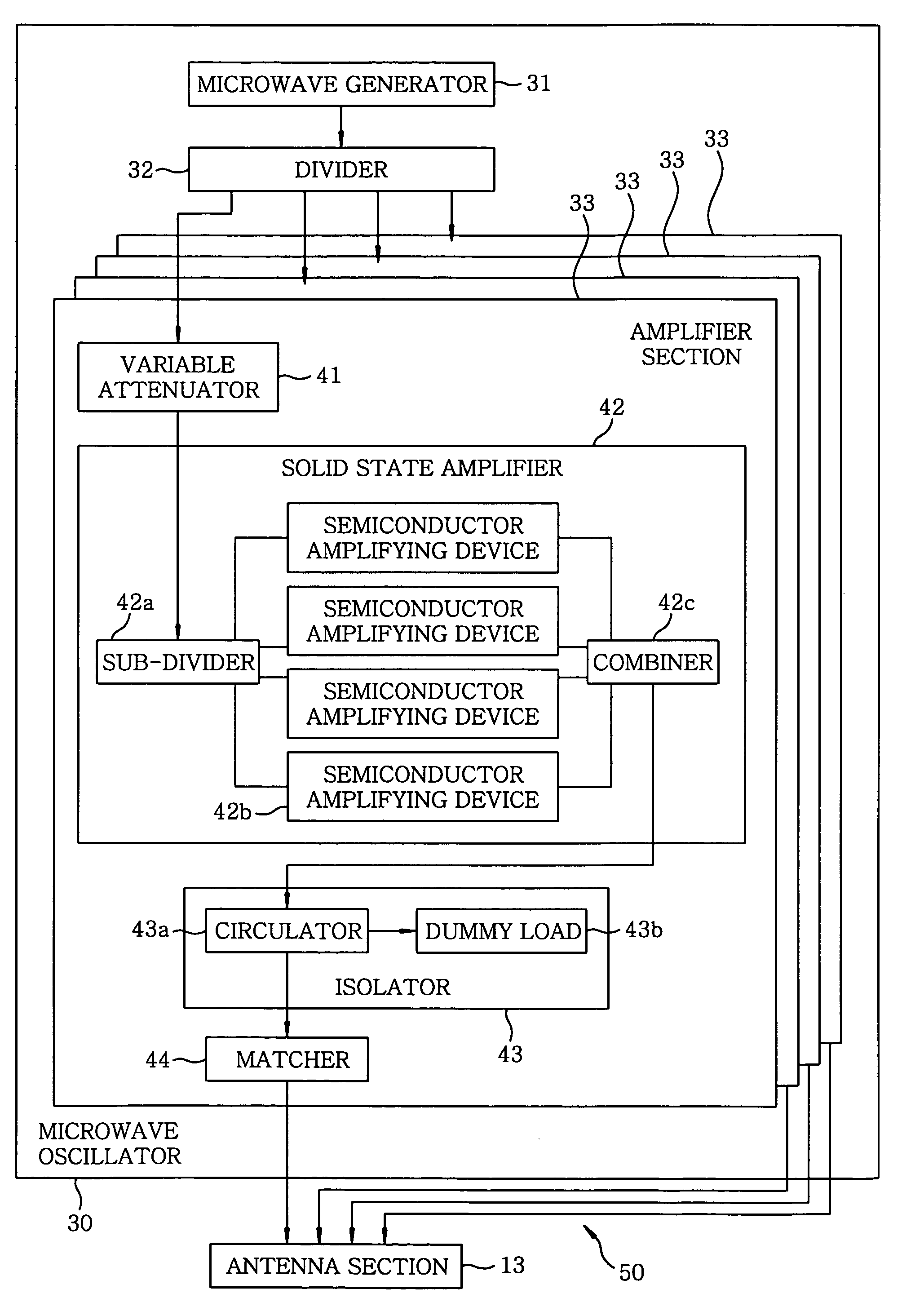
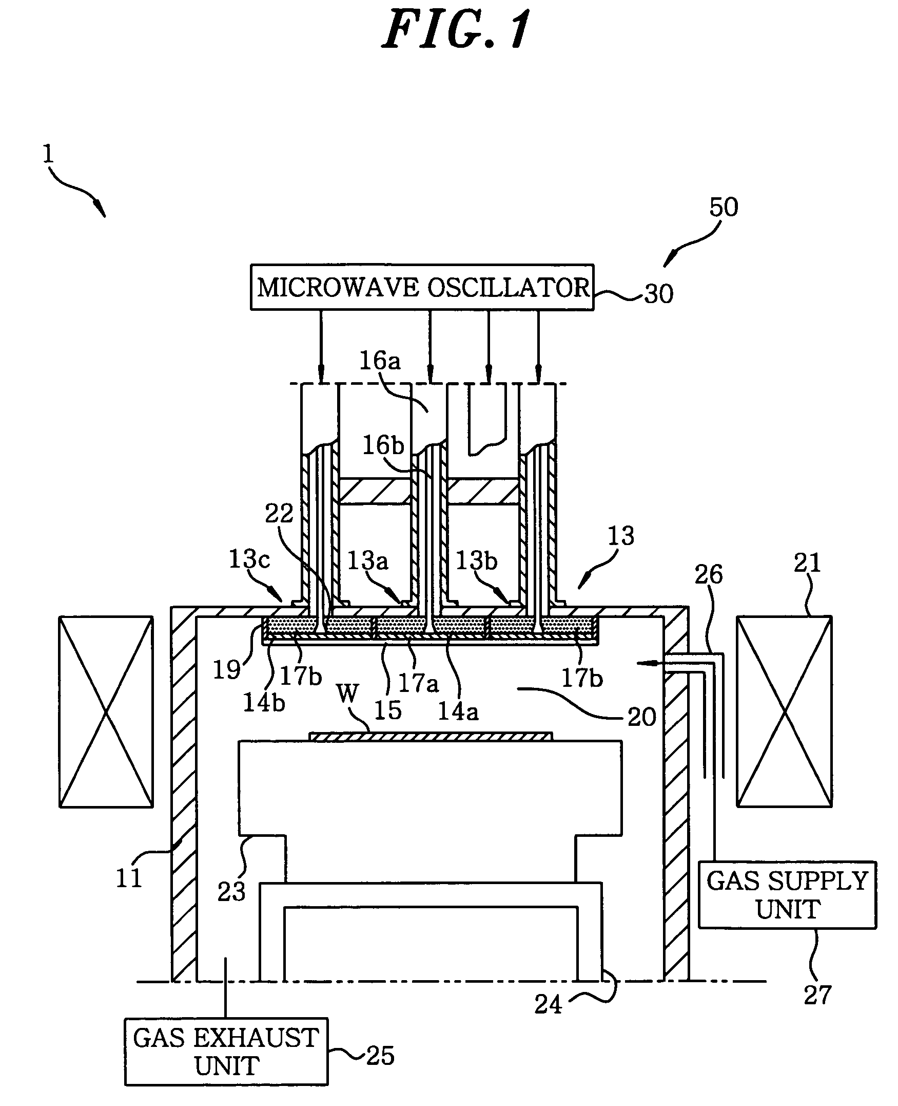
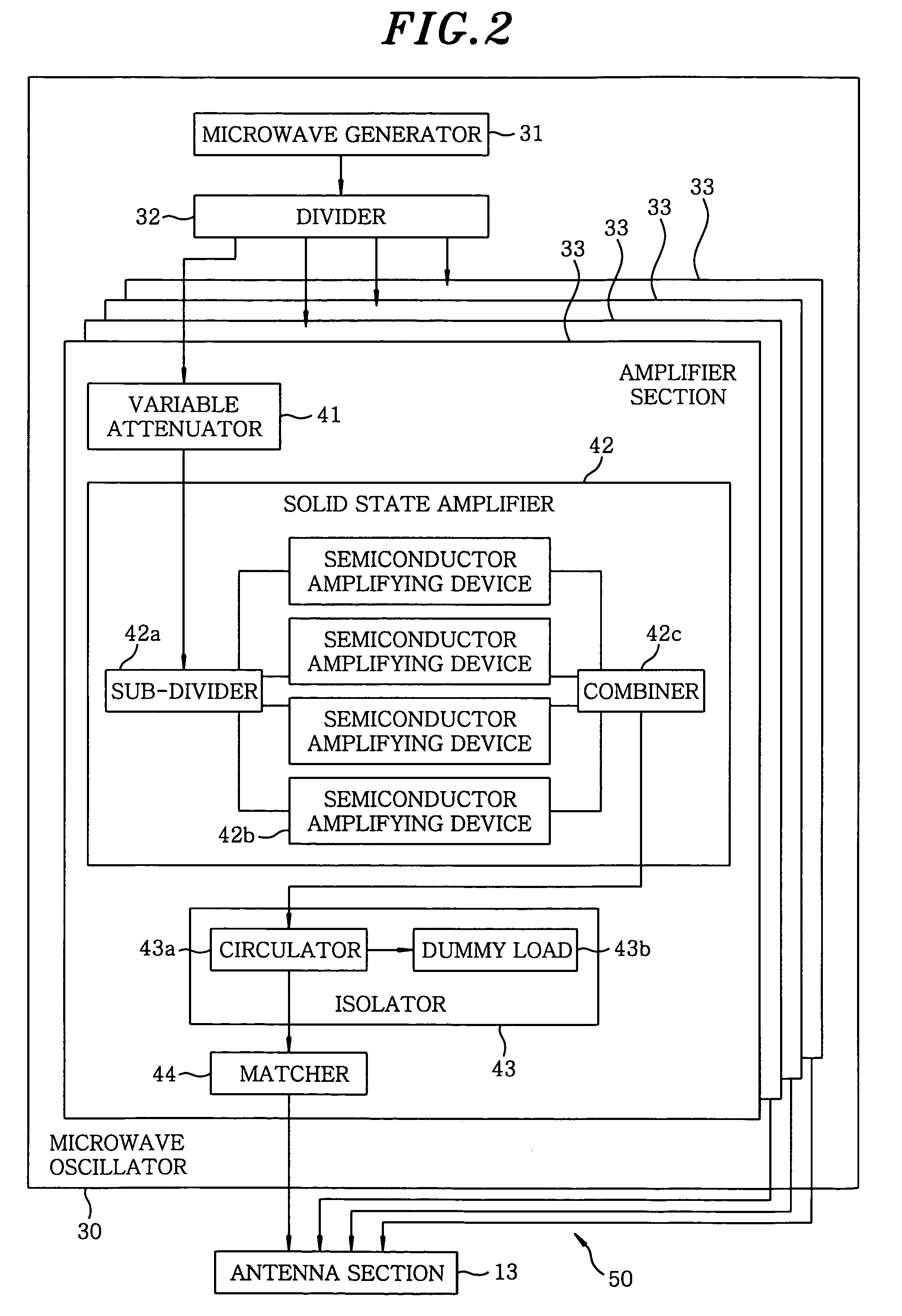
[0037]Hereinafter, preferred embodiments of the present invention will be described with reference to the accompanying drawings. FIG. 1 shows a schematic cross sectional view of a plasma etching apparatus 1 as an example of a plasma processing apparatus. FIG. 2 is an explanatory diagram showing a detailed configuration of a microwave introducing unit 50 installed in the plasma etching apparatus 1. Further, in the plasma etching apparatus 1, a substrate to be processed is a semiconductor wafer W.

[0038]The plasma etching apparatus 1 includes a chamber 11 for containing the wafer W therein; a gas inlet opening 26 provided in the chamber 11; a gas supply unit 27 which supplies a processing gas (e.g., Cl2) for producing a plasma into the chamber 11 through the gas inlet opening 26; a gas exhaust port 24 installed in the chamber 11; a gas exhaust unit 25 for exhausting an inside of the chamber 11 through the gas exhaust port 24; a substrate support stage 23 for supporting the wafer W in t...


PUM

PropertyMeasurementUnit
frequencyaaaaaaaaaa
poweraaaaaaaaaa
poweraaaaaaaaaa

Abstract

A plasma processing apparatus includes a chamber for containing a substrate to be processed, a gas supply unit for supplying a processing gas into the chamber, and a microwave introducing unit for introducing plasma generating microwaves into the chamber. The microwave introducing unit includes a microwave oscillator for outputting a plurality if microwaves having specified outputs, and an antenna section having a plurality of antennas to which the microwaves outputted from the microwave oscillator are respectively transmitted.

Description

[0001]This application is a Continuation Application of PCT International Application No. PCT / JP03 / 12792 filed on Oct. 6, 2003, which designated the United States.FIELD OF THE INVENTION[0002]The present invention relates to a plasma processing apparatus for performing a plasma process such as an etching on a substrate to be processed.BACKGROUND OF THE INVENTION[0003]In a manufacturing process of a semiconductor device or a liquid crystal display device, a plasma processing apparatus such as a plasma etching apparatus and a plasma CVD film forming apparatus has been employed to perform a plasma process, e.g., an etching process or a film forming process, on a substrate to be processed such as a semiconductor wafer and a glass substrate.[0004]There are well-known plasma generating methods used in the plasma processing apparatus, e.g., a method including steps of supplying a processing gas into a chamber with parallel plate electrodes disposed therein; feeding a specific power to the p...

Claims


Application Information

Patent Timeline
Patent Type & Authority Patents(United States)
IPC IPC(8): C23C16/00H01L21/306C23F1/00
CPCH05B6/705
Inventor KASAI, SHIGERUOSADA, YUKIOGINO, TAKASHI
Owner COMMSCOPE TECH LLC
Why Eureka
Try Eureka