Method and structure for fabricating mechanical mirror structures using backside alignment techniques

a mechanical mirror and alignment technique technology, applied in the field of backside alignment techniques, can solve the problems of difficult to make larger, low yield of liquid crystal panels, and large volume of crts, and achieve the effects of improving integrated structure, high device yield, and convenient us

Inactive Publication Date: 2008-11-11
MIRADIA INC
View PDF64 Cites 2 Cited by
  • Summary
  • Abstract
  • Description
  • Claims
  • Application Information

AI Technical Summary

Benefits of technology

[0009]Many benefits are achieved by way of the present invention over conventional techniques. For example, the present technique provides an easy to use process that relies upon conventional technology. In some embodiments, the method provides higher device yields for the bonded substrates. Additionally, the method provides a process that is compatible with conventional process technology without substantial modifications to conventional equipment and processes. Preferably, the invention provides for an improved integrated structure including integrated circuits and mirror structures for display applications. Preferably, the present method can be used to see alignment marks through a thickness of silicon bearing material such as a silicon wafer. More preferably, the invention includes a method for aligning a photomask onto a backside of a multilayered substrate structure using an alignment mark within a thickness of the multilayered alignment mark, which is accurate and easy to process. The method provides an accurate alignment technique of 200 nanometers and less using standard lithography tools. Depending upon the embodiment, one or more of these benefits may be achieved. These and other benefits will be described in more throughout the present specification and more particularly below.

Problems solved by technology

Although very successful, CRTs were often bulky, difficult to make larger, and had other limitations.
Unfortunately, liquid crystal panels often had low yields and were difficult to scale up to larger sizes.
These LCDs were often unsuitable for larger displays often required for television sets and the like.
Although DLP has been successful, it is often difficult to manufacture and subject to low yields, etc.
Additionally, DLP relies upon non-standard MEMS based manufacturing techniques, which are often not reliable and lead to increased costs.

Method used


Image

  • Method and structure for fabricating mechanical mirror structures using backside alignment techniques
  • Method and structure for fabricating mechanical mirror structures using backside alignment techniques
  • Method and structure for fabricating mechanical mirror structures using backside alignment techniques

Examples


Embodiment Construction

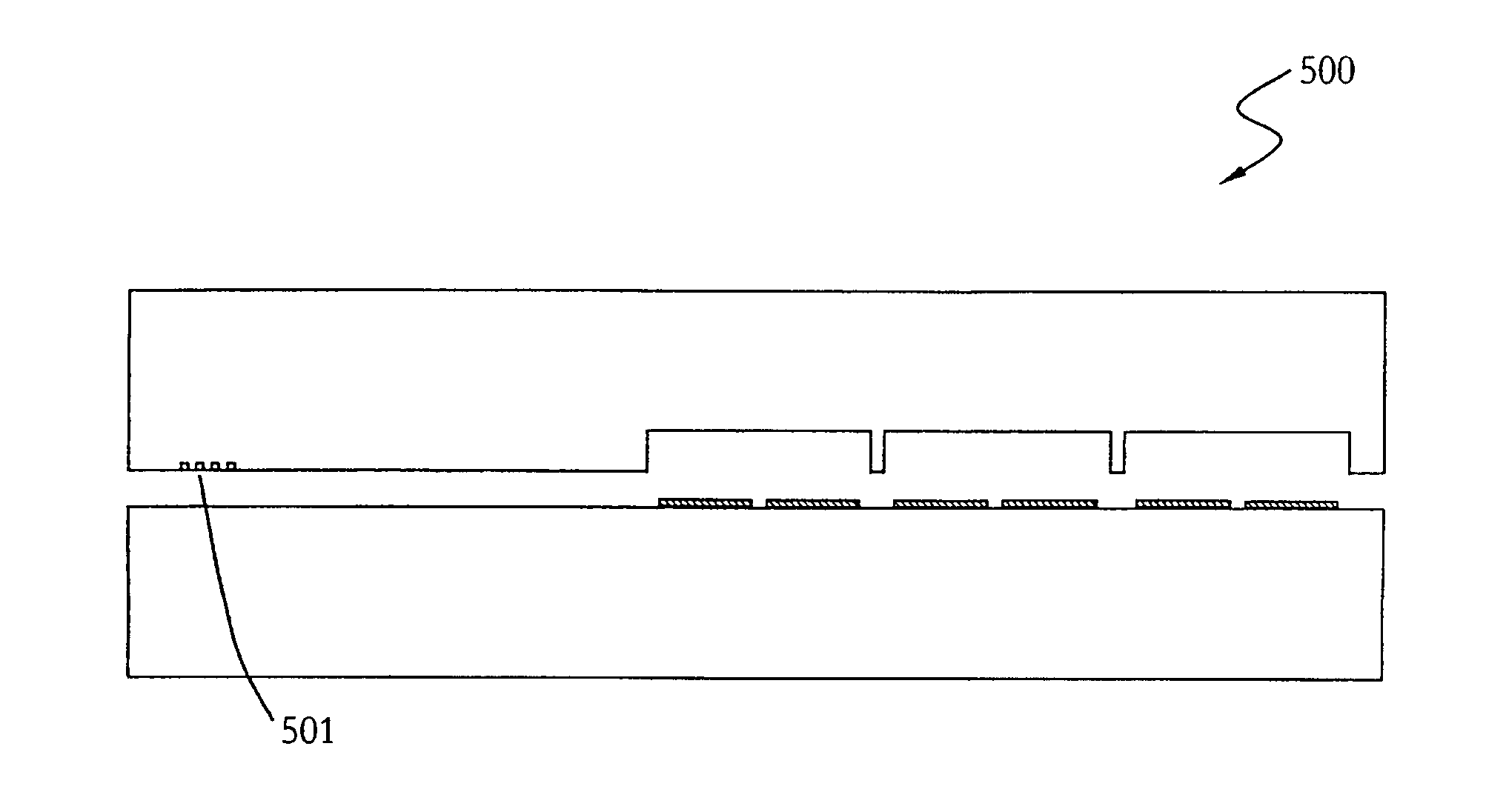
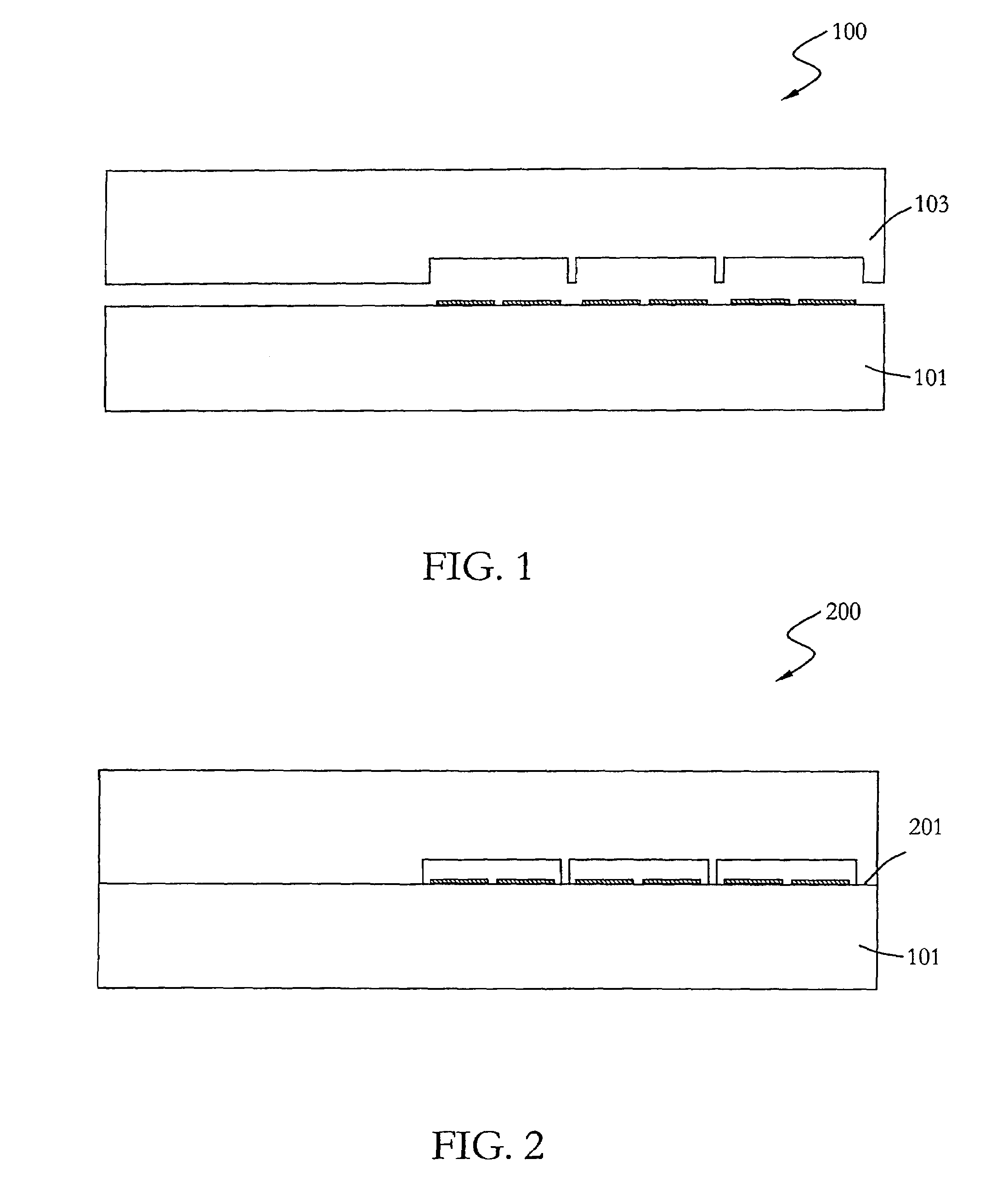
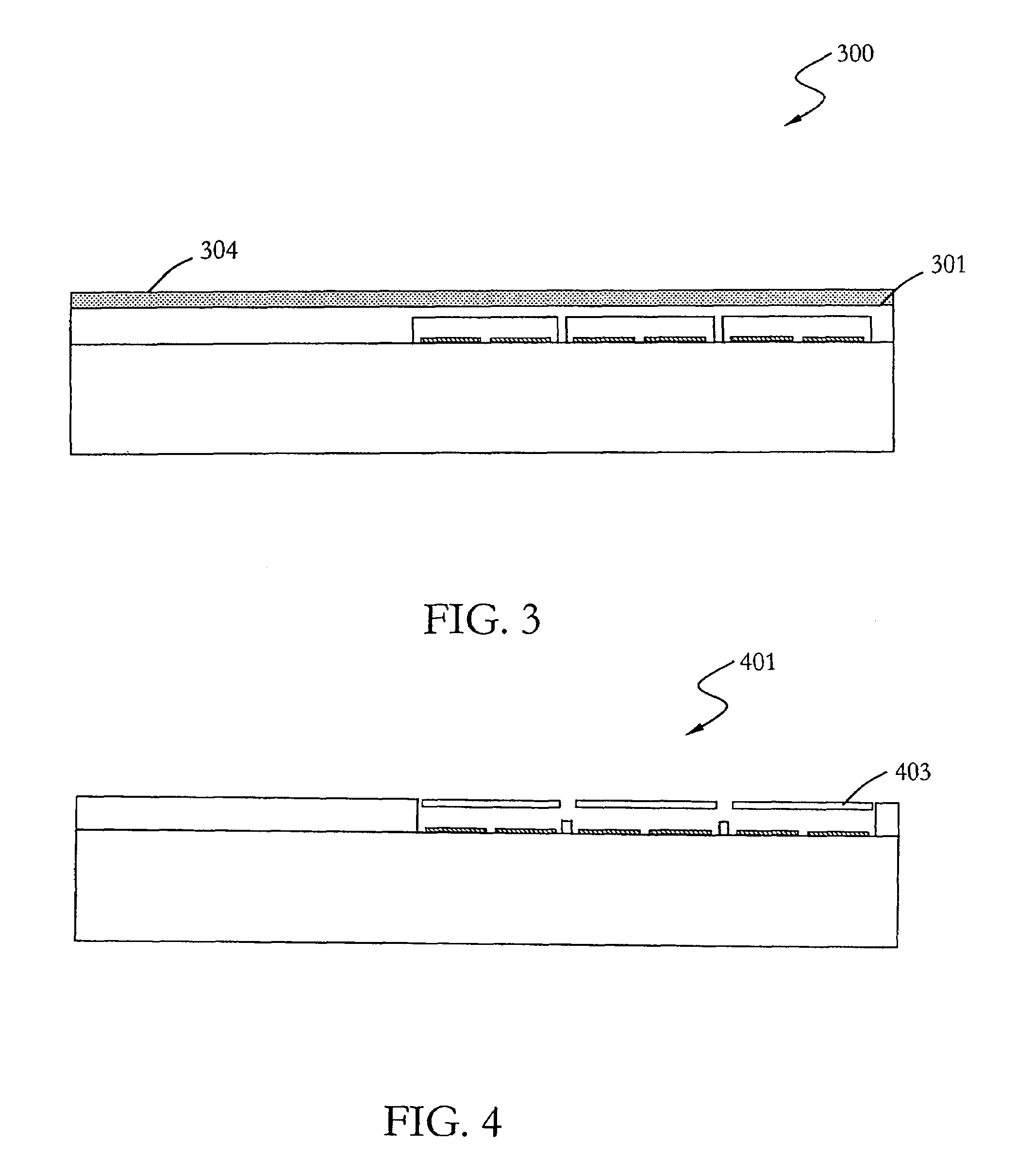
[0014]According to the present invention, techniques for bonding substrates are provided. More particularly, the invention includes a method and structure for bonding substrates together using alignment marks. Merely by way of example, the invention has been applied to integrating a mechanical based structure with an integrated circuit chip. But it would be recognized that the invention has a much broader range of applicability.

[0015]In a specific embodiment, a method for fabricating mechanical structures from bonding substrates can be summarized as follows.

[0016]1. Provide a first substrate having a first thickness of silicon material and a first face.

[0017]2. Provide a second substrate having a second thickness and a second face.

[0018]3. Bond the first face of the first substrate with the second face of the second substrate.

[0019]4. Expose an alignment mark comprising a front-size zero mark within a portion of either the first thickness or the second thickness.

[0020]5. Apply a lay...


PUM

PropertyMeasurementUnit
thicknessaaaaaaaaaa
thicknessaaaaaaaaaa
depthaaaaaaaaaa

Abstract

A method for fabricating mechanical structures from bonding substrates. The method includes providing a bonded substrate structure, which includes a first substrate having a first thickness of silicon material and a first face. The bonded substrate also includes a second substrate having a second thickness and a second face. At least the first substrate or at least the second substrate (or both) has an alignment mark comprising a front-size zero mark within a portion of either the first thickness or the second thickness. The method includes applying a layer of photomasking material overlying a first backside surface of the first substrate. The method includes illuminating electromagnetic radiation using a coherent light source through the layer of photoresist material and through a portion of the first thickness. The method includes detecting an indication of the alignment mark using a signal associated with a portion of the electromagnetic radiation from a second backside of the second substrate. The method also includes exposing a portion of the layer of photomasking material once a pattern a portion of a reticle structure has been aligned using the alignment mark.

Description

BACKSIDE ALIGNMENT TECHNIQUES[0001]The present invention relates generally to bonding techniques. More particularly, the invention includes a method and structure for bonding substrates together using alignment marks. Merely by way of example, the invention has been applied to integrating a mechanical based structure with an integrated circuit chip. But it would be recognized that the invention has a much broader range of applicability.[0002]Visual display technologies have rapidly developed over the years. Most particularly, electronic displays for outputting television shows, streaming video, and the like. From the early days, cathode ray tube technology, commonly called CRTs, outputted selected pixel elements onto a glass screen in conventional television sets. These television sets originally output black and white moving pictures. Color television sets soon replaced most if not all black and white television units. Although very successful, CRTs were often bulky, difficult to m...

Claims


Application Information

Patent Timeline
Patent Type & Authority Patents(United States)
IPC IPC(8): G03F7/00
CPCB81C1/00484B81C2203/036B81C2203/051
Inventor YANG, XIAO CHARLES
Owner MIRADIA INC
Why Eureka
Try Eureka