Liquid crystal display device with plurality of interconnected island shaped pixel portions forming pixel electrodes where scanning line overlaps an interconnected portion

a liquid crystal display and interconnected technology, applied in non-linear optics, instruments, optics, etc., can solve the problems of reduced aperture ratio, narrow viewing angle of transmissive display, low degree of flexibility in optical design, etc., to prevent alignment disorder, high aperture ratio, and sufficient layout space

Active Publication Date: 2008-11-11
BOE TECH GRP CO LTD
View PDF7 Cites 23 Cited by
  • Summary
  • Abstract
  • Description
  • Claims
  • Application Information

AI Technical Summary

Benefits of technology

[0011]An advantage of the invention is that it provides a transflective liquid crystal display device capable of ensuring a sufficient space for the layout below a reflective film even if the structure is complicated, while maintaining a high aperture ratio, and of preventing alignment disorder caused by contact holes.
[0012]According to an aspect of the invention, a liquid crystal display device includes an element substrate, a counter substrate, a liquid crystal layer, first and second dot sections, an insulating film, and a switching element. Each of the dot sections includes a pixel electrode with a transmissive display portion where transmissive display of the dot section is performed and a reflective display portion where reflective display of the dot section is performed. The insulating film is disposed between the liquid crystal layer on one side and the first and second pixel electrodes on the other. The switching element is disposed between the liquid crystal layer and the insulating film and electrically connected to the first pixel electrode through a contact hole in the insulating film. The switching element is located at a position that overlaps the reflective display portion of the second pixel electrode in plan view.
[0013]According to this structure, since the switching element is provided in a different dot region, a sufficient space for the layout is ensured below the reflective electrode portion, and thus the degree of flexibility of the design of the dot region is improved. Accordingly, although the structure becomes complicated, an aperture ratio is not reduced. In addition, since the switching element and the contact hole are arranged in different dot regions, the contact hole can be provided closer to the edge of the dot region, which makes it possible to reduce the effects of alignment disorder on liquid crystal due to the contact hole.
[0014]Further, in the above-mentioned structure, it is preferable that the contact hole be provided at an edge portion of the pixel electrode, particularly, at a corner of the pixel electrode.
[0015]According to this structure, it is possible to reduce the effects of alignment disorder due to the contact hole to the minimum.
[0016]Furthermore, in the above-mentioned structure, it is preferable that the element substrate further include electrode lines connected to the switching elements, and that each electrode lines be arranged below the reflective electrode portion of the second dot region.

Problems solved by technology

However, this type of transflective liquid crystal display device has a problem in that a viewing angle is narrow in the transmissive display.
The reason is that, since the transflective plate is provided on an inner surface of a liquid crystal cell to prevent the occurrence of parallax, reflective display should be performed by using only one polarizing plate provided on an observer side, which results in a low degree of flexibility in the optical design.
However, it is difficult to form both the switching element and the contact hole below the reflective film as the structure becomes more complicated, which results in a reduction in aperture ratio.

Method used


Image

  • Liquid crystal display device with plurality of interconnected island shaped pixel portions forming pixel electrodes where scanning line overlaps an interconnected portion
  • Liquid crystal display device with plurality of interconnected island shaped pixel portions forming pixel electrodes where scanning line overlaps an interconnected portion
  • Liquid crystal display device with plurality of interconnected island shaped pixel portions forming pixel electrodes where scanning line overlaps an interconnected portion

Examples


first embodiment

[0030]Liquid Crystal Display Device

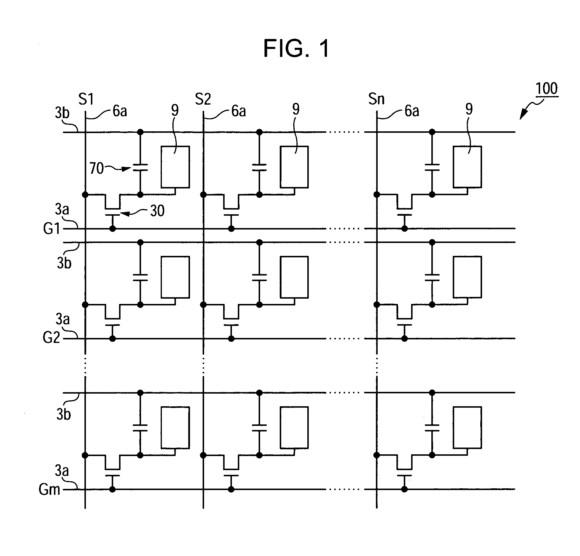
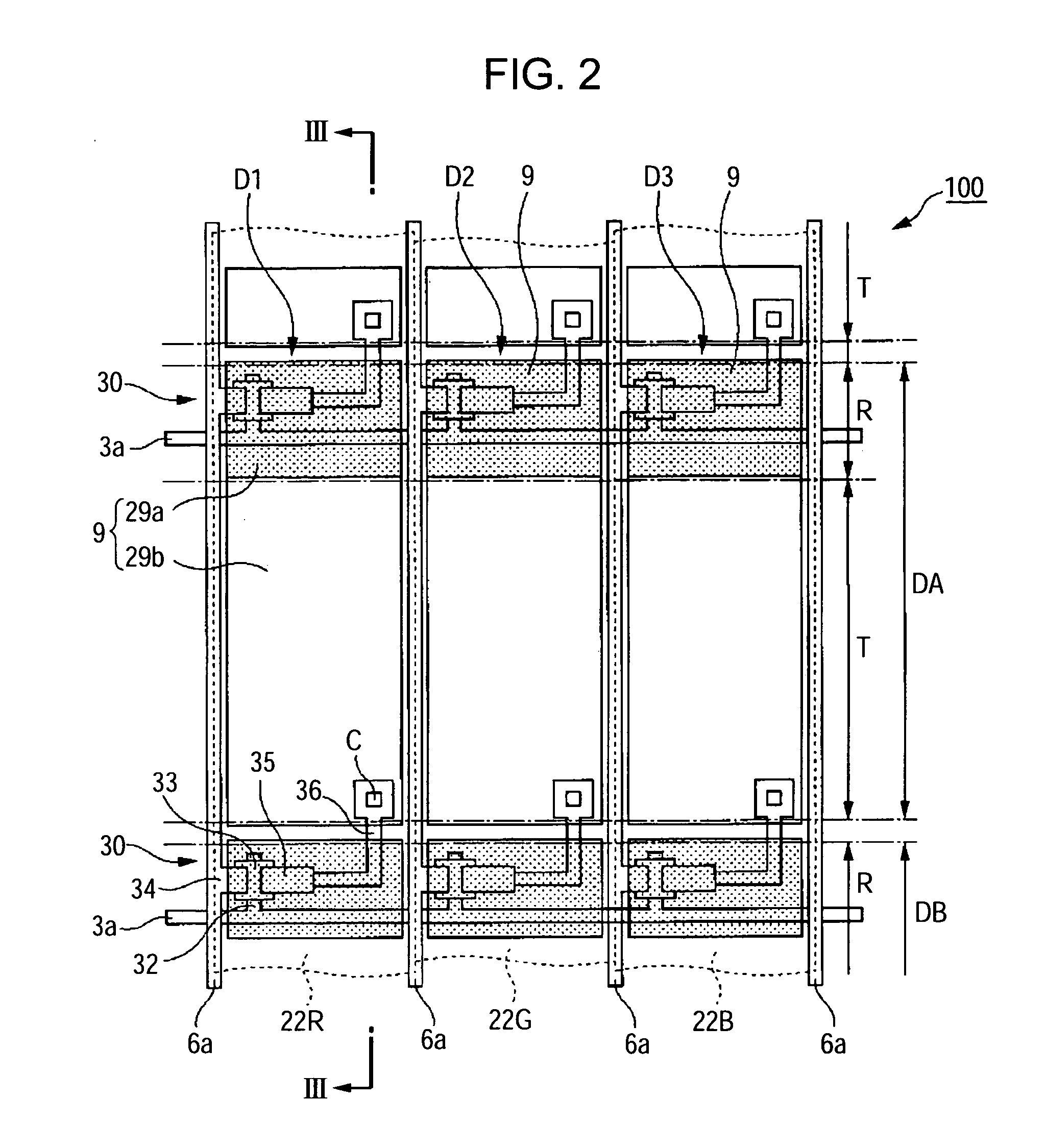
[0031]FIG. 1 is an equivalent circuit diagram of a plurality of dots arranged in a matrix that constitute an image display region of a liquid crystal display device according to a first embodiment of the invention, and FIG. 2 is a plan view illustrating the structure of a pixel region of the liquid crystal display device of the first embodiment. FIG. 3 is a partially cross-sectional view illustrating the structure of the liquid crystal display device, and is taken along the line III-III of FIG. 2.

[0032]A liquid crystal display device 100 of this embodiment is an active-matrix transflective liquid crystal device that uses thin film transistors (TFTs) as switching elements. In the liquid crystal display device 100 of this embodiment, as shown in FIG. 1, each of the plurality of dots arranged in a matrix that constitute the image display region includes a pixel electrode 9 and a TFT 30 serving as a switching element to control the pixel electrode 9. A...

second embodiment

[0048]Liquid Crystal Display Device

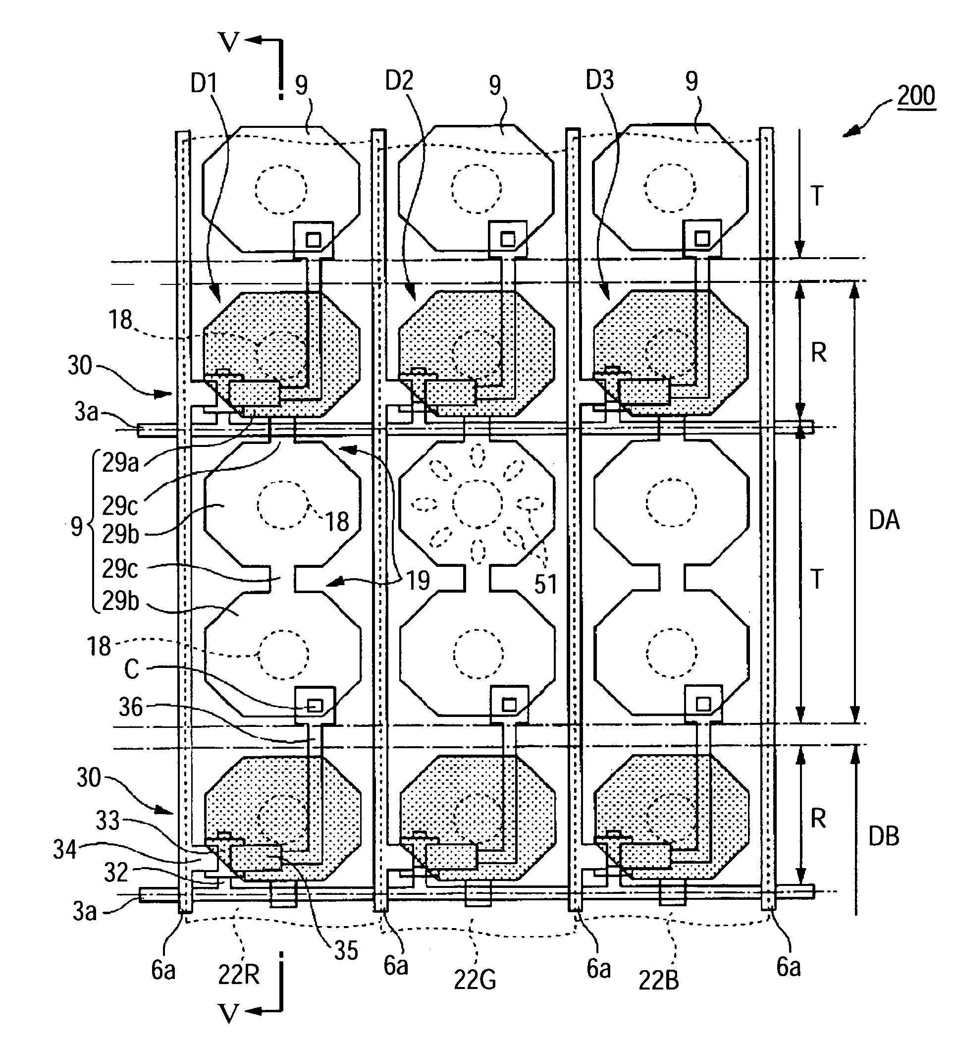
[0049]Next, a second embodiment of the invention will be described. FIG. 4 is a plan view illustrating the structure of one pixel region of a liquid crystal display device 200 according to the second embodiment of the invention. FIG. 5 is a partially cross-sectional view illustrating the structure of the liquid crystal display device, taken along the line V-V of FIG. 4. In this embodiment, the same components as those in the first embodiment have the same reference numerals, and a description thereof will be omitted.

[0050]The second embodiment is different from the first embodiment in that a vertical alignment mode is used as a liquid crystal mode, in that the pixel electrode 9 in one dot region is divided into a plurality of island-shaped sub-pixels, and dielectric projections 18 for regulating the alignment of liquid crystal are provided on a counter substrate, corresponding to the respective sub-pixels, and in that the arrangement of the scannin...


PUM

PropertyMeasurementUnit
twist angleaaaaaaaaaa
thicknessaaaaaaaaaa
thicknessaaaaaaaaaa

Abstract

A liquid crystal display device includes an element substrate; a counter substrate opposite to the element substrate; a liquid crystal layer that is formed between the element substrate and the counter substrate; and dot sections each having a transmissive display section for performing transmissive display and a reflective display section for performing reflective display. The element substrate includes switching elements, an insulating film formed on the switching elements, and pixel electrodes formed on the insulating film. The switching elements are electrically connected to the pixel electrodes through contact holes that are formed in the insulating film. Each of the pixel electrodes has a transparent electrode portion for the transmissive display and a reflective electrode portion for the reflective display. The switching element is arranged below the reflective electrode portion of a second dot section adjacent to a first dot section that is driven by the switching element.

Description

RELATED APPLICATION[0001]This application claims priority to Japanese Patent Application No. 2004-256810 filed Sept. 3, 2004 which is hereby expressly incorporated by reference herein in its entirety.BACKGROUND OF THE INVENTION[0002]1. Technical Field[0003]The present invention relates to a transflective liquid crystal display device in which one dot region includes a reflective display region and a transmissive display region and to an electronic apparatus including the same.[0004]2. Related Art[0005]Transflective liquid crystal display devices having both a reflective mode and a transmissive mode have been generally known as liquid crystal display devices. As the transflective liquid crystal display device, a display device has been suggested in which a liquid crystal layer is interposed between an upper substrate and a lower substrate, and a reflective film obtained by forming light-transmissive windows in a metal film made of, for example, Al is provided on an inner surface of t...

Claims


Application Information

Patent Timeline
Patent Type & Authority Patents(United States)
IPC IPC(8): G02F1/1335
CPCG02F1/133555G02F1/133707G02F1/134309G02F1/1362G02F1/1393G02F1/1335
Inventor TSUCHIYA, HITOSHI
Owner BOE TECH GRP CO LTD
Why Eureka
Try Eureka