Bit line setup and discharge circuit for programming non-volatile memory

a non-volatile memory and programming technology, applied in static storage, digital storage, instruments, etc., can solve the problems of large transient noise peak, more noise in the power supply voltage vcc or ground voltage, and program inhibition, so as to reduce power and ground noise and limit peak current

Inactive Publication Date: 2008-11-18
SAMSUNG ELECTRONICS CO LTD
View PDF45 Cites 28 Cited by
  • Summary
  • Abstract
  • Description
  • Claims
  • Application Information

AI Technical Summary

Benefits of technology

[0024]In accordance with the invention, disclosed circuits and methods reduce the power and ground noise that occur when charging bit lines up to supply voltage Vcc or discharging the bit lines to ground (0V). In particular, one embodiment of the invention is a NAND EEPROM having a shielded bit line architecture. This NAND EEPROM has a virtual power node that is connected to bit lines for charging or discharging of the bit lines. A PMOS pull-up transistor and an NMOS pull down transistor connect to the virtual power node, and a control circuit for charging or discharging bit lines controls the gate voltages of the PMOS pull-up transistor and the NMOS pull-down transistor to limit peak current when charging or discharging bit lines. In particular, the control circuit operates the PMOS or NMOS transistor in a non-saturation mode to limit current. One such control circuit creates a current mirror or applies a reference voltage to control gate voltages.

Problems solved by technology

However, program inhibition in the shielded bit line architecture charges bit lines assigned to a non-selected page (hereinafter referred to as “shielded bit lines”) and bit lines connected to memory cell that are in a selected page but not to be programmed.
As circuit density, data access rates, and required charging and discharging capacities increase, bit line setup and bit line discharge cause more noise in the power supply voltages Vcc or the ground voltage.
In particular, the rapid switching when driving virtual power node VIRPWR to supply voltage Vcc or ground creates a large transient noise peak.
Such noise concerns are likely to worsen as the memory circuit densities increase since the bit line setup raises half of the bit lines (the even-numbered or the odd-numbered) to supply voltage Vcc before programming.

Method used


Image

  • Bit line setup and discharge circuit for programming non-volatile memory
  • Bit line setup and discharge circuit for programming non-volatile memory
  • Bit line setup and discharge circuit for programming non-volatile memory

Examples


Embodiment Construction

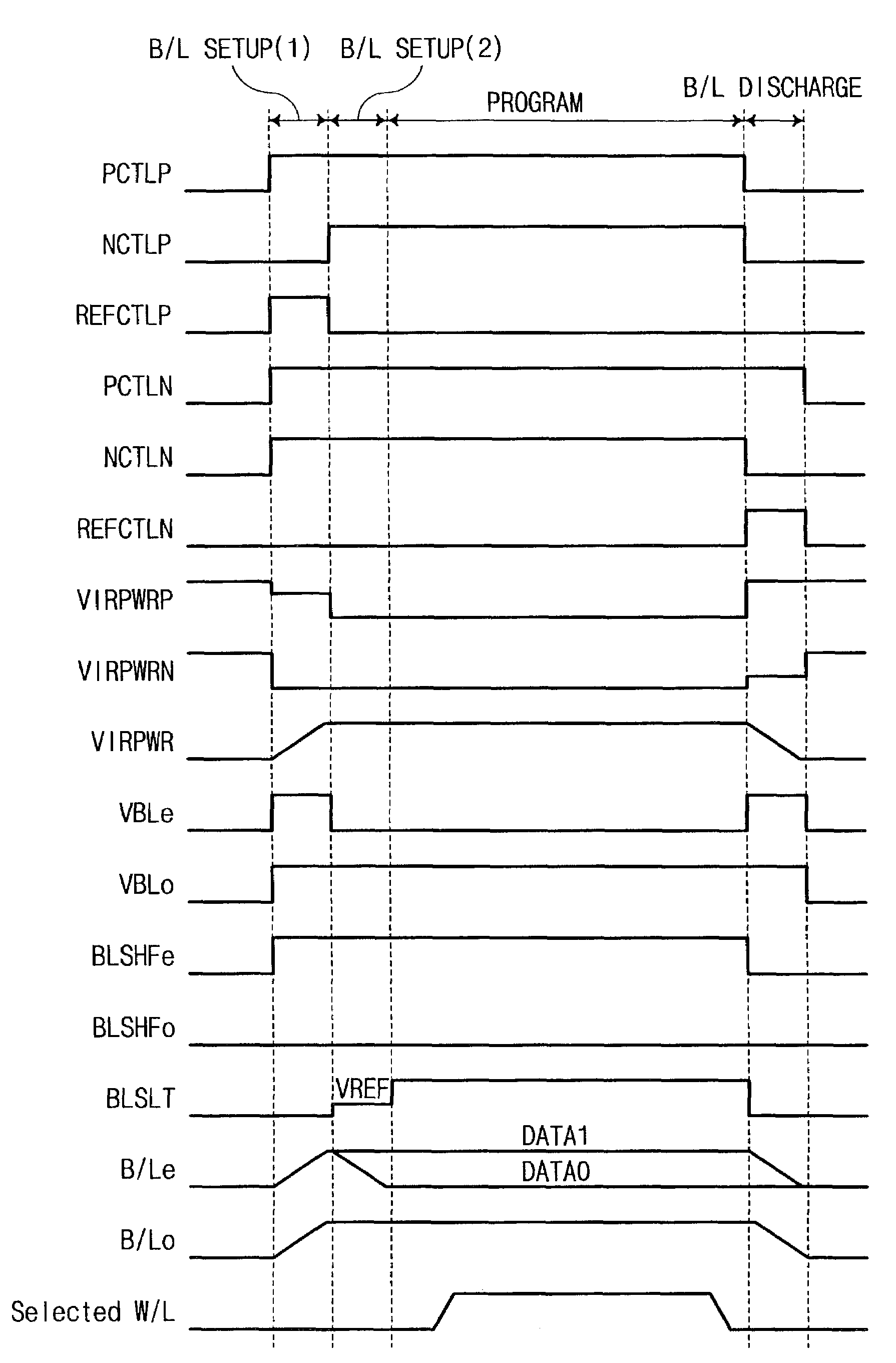
[0048]In accordance with an aspect of the present invention, transistors biased to conduct less than a saturation current can reduce noise in supply and ground voltages by reducing the peak currents during charging or discharging of bit lines for a programming operation.

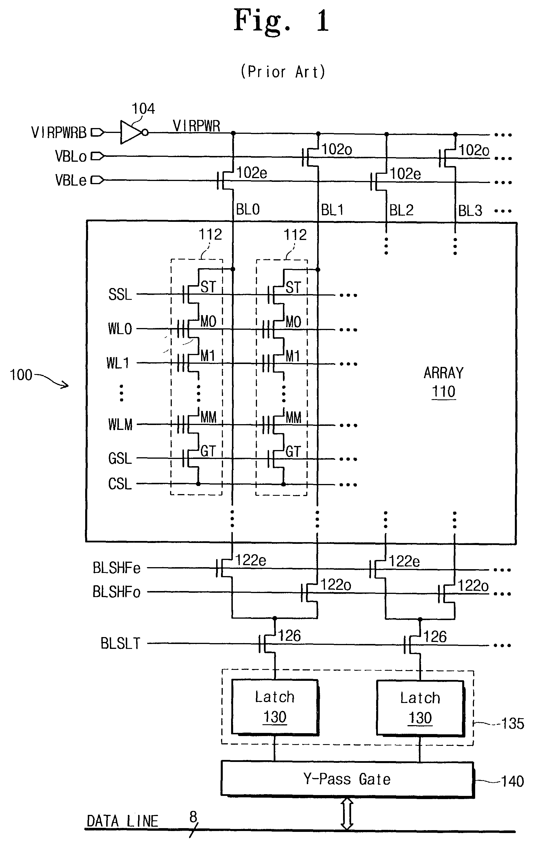
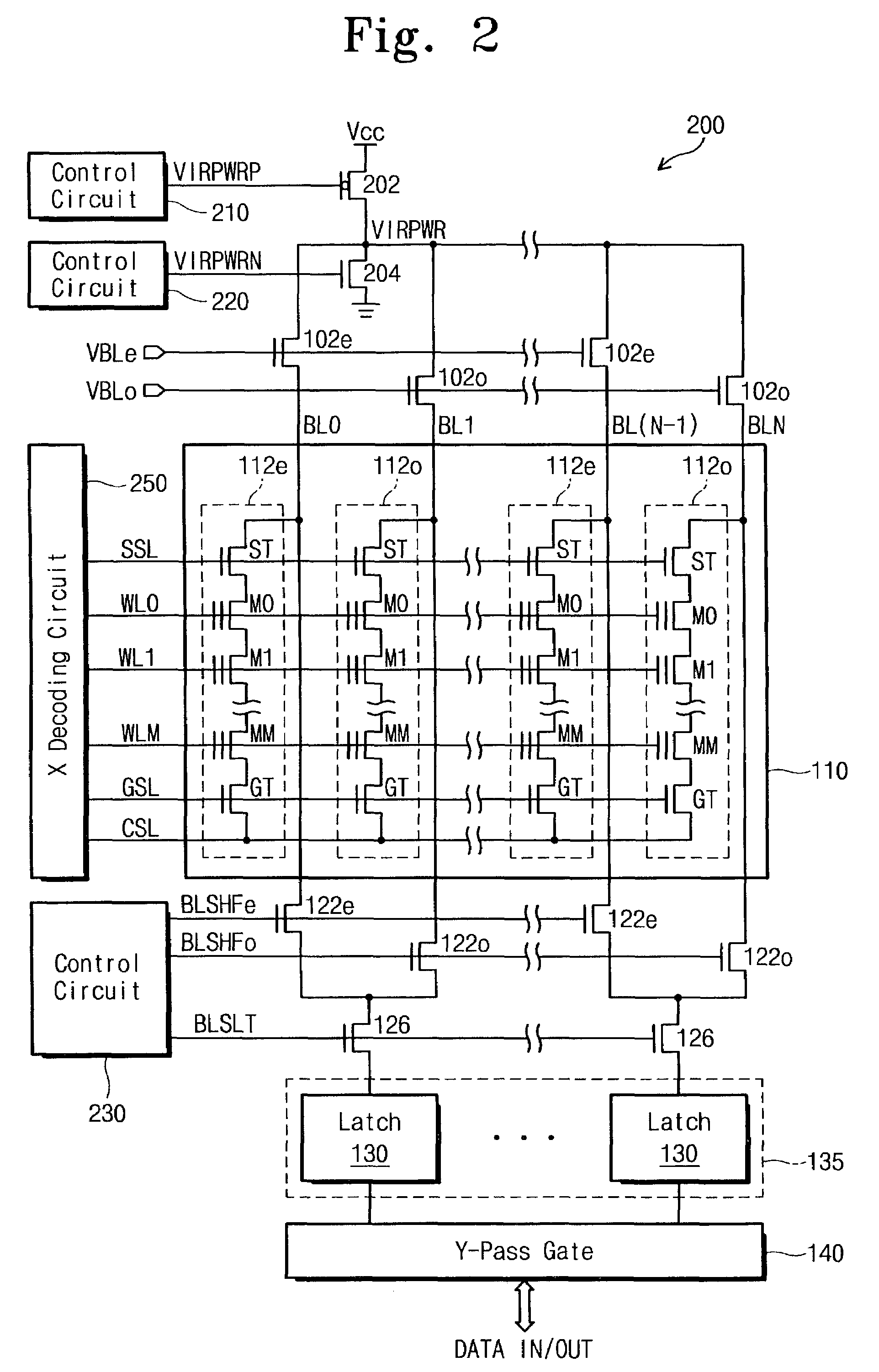
[0049]FIG. 2 shows a NAND flash EEPROM 200 according to an embodiment of the invention that reduces the peak current when charging or discharging bit lines. NAND flash EEPROM 200 includes a cell array 110, which can be a conventional NAND array such as described above in regard to FIG. 1. In particular, cell array 110 includes NAND strings 112 attached to bit lines BL0 to BLN. Although FIG. 2 shows only a single NAND string 112 coupled to each bit line, a typical embodiment would have multiple NAND strings coupled to each bit line.

[0050]Each NAND string 112 includes first and second select transistors ST and GT and M+1 cell transistors M0 to MM, which are connected in series. Each first select transistor has a drain ...


PUM


Abstract

A NAND EEPROM having a shielded bit line architecture reduces supply voltage and ground noise resulting from charging or discharging bit lines. The EEPROM has a PMOS pull-up transistor and an NMOS pull down transistor connected to a virtual power node. A control circuit for charging or discharging bit lines controls the gate voltage of the PMOS or NMOS transistor to limit peak current when charging or discharging bit lines via the virtual power node. In particular, the control circuit operates the PMOS or NMOS transistor in a non-saturation mode to limit current. One such control circuit creates a current mirror or applies a reference voltage to control gate voltages. A programming method sets up bit lines by pre-charging unselected bit lines via the PMOS pull-up transistor having controlled gate voltage while latches in the programming circuitry charge or discharge selected bit lines according to respective data bits being stored. Another bit line setup includes two stages. A first stage pre-charges all bit lines via PMOS pull-up, and the second stage uses the latches to discharge or leave charged the selected bit lines depending on respective data bits being stored. The gate voltages of NMOS transistors in the programming circuitry can be controlled to reduce noise caused by discharging selected bit lines through the latches.

Description

CROSS-REFERENCE TO RELATED APPLICATION[0001]This application is a divisional of U.S. patent application Ser. No. 09 / 791,473, filed Feb. 22, 2001 now U.S. Pat. No. 6,480,419.BACKGROUND[0002]1. Field of the Invention[0003]This invention relates to nonvolatile semiconductor memory devices and write or programming processes for nonvolatile semiconductor memory devices.[0004]2. Description of Related Art[0005]EEPROMs, unlike many other nonvolatile memories, can electrically erase old data and write new data. This flexibility in data management makes EEPROMs the preferred nonvolatile memory in system programming, where data may be refreshed and must be available when a system powers up.[0006]A conventional memory cell in an EEPROM includes an N-channel cell transistor, which has a floating gate over a channel region defined between N+ source and drain in a P-type substrate, and a control gate overlying the floating gate. The floating and control gates are made out of a conductive material...

Claims


Application Information

Patent Timeline
Patent Type & Authority Patents(United States)
IPC IPC(8): G11C11/34G11C16/02G11C16/06G11C16/04G11C16/10G11C16/24G11C16/30
CPCG11C16/10G11C16/24G11C16/30G11C16/06
Inventor LEE, YEONG-TAEK
Owner SAMSUNG ELECTRONICS CO LTD
Why Eureka
Try Eureka