Semiconductor package having a grid array of pin-attached balls

a technology of pin-attached balls and semiconductors, which is applied in the direction of printed electric component incorporation, sustainable manufacturing/processing, and final product manufacturing, etc., can solve the problems of difficult routing of ball grid array packages, unfavorable high frequency lines, and lack of uniformity, so as to achieve high input/output ratio, high density, and high density

Active Publication Date: 2008-12-09
TEXAS INSTR INC
View PDF17 Cites 10 Cited by
  • Summary
  • Abstract
  • Description
  • Claims
  • Application Information

AI Technical Summary

Benefits of technology

[0006]This invention addresses the need for a coherent concept of ball grid package structure and fabrication method, how to assemble high lead count and preferably chip-scale devices. Packages based on this concept as disclosed by the present invention provide excellent electrical performance, mechanical stability, and high product reliability. It is a technical advantage of the invention that the fabrication method is flexible enough to be applied for different semiconductor product families and a wide spectrum of design and process variations. It is further an advantage that the innovations can be accomplished while shortening production cycle time and increasing throughput.
[0007]One embodiment of the invention is a substrate for the assembly of semiconductor devices. The substrate has first and second surfaces and comprises a sheet-like base of insulating material, preferably compliant. A plurality of connecting lines are on the first substrate surface, selected lines interconnecting conductive members, preferably rings, and terminals. A conductive pin, having a head on one end, is in each of these members so that the pin extends through the substrate base and protrudes from the second surface, while its head rests on its respective member. The protruding pin has a surface composition metallurgically suitable for solder attachment.
[0008]Another embodiment of the invention is a semiconductor assembly with a substrate as described above and an integrated circuit chip with its contact pads connected to the substrate terminals. The conductive pins extending through the substrate have a separate body of solder material attached to their protruding ends, providing strong mechanical solder attachment. Since the pins anchoring of the solder bodies require much less substrate area than the traditional solder-on-metal joints, these area savings can now be devoted to more generous interconnecting line layouts.
[0009]Another embodiment of the invention is a method for fabricating a substrate for the assembly of semiconductor devices. First, a sheet-like base of insulating material is provided, the base having first and second surfaces. Then, a plurality of connecting lines is formed on the first surface so that selected lines interconnect conductive members and terminals. Finally, a conductive pin, having a head on one end, is inserted in each of the members so that the pin penetrates through the base until it protrudes from the second surface and the pin head rests on the member. It is preferable for some base materials to heat the sheet-like base approximately to the temperature of the elastic limit of the material, before the pins are inserted and pushed through.
[0010]In another embodiment of the invention, a semiconductor device is assembled by providing the substrate with the pins as described above and further providing an integrated circuit chip having contact pads. The contact pads and the substrate terminals are connected, respectively, either by wire bonding or by bump bonding. A separate body of solder material is attached to each protruding pin, preferably so that the pin penetrates the solder body at least halfway. A preferred attachment method aligns the solder material with respect to the protruding substrate pins, applies thermal energy to reach the solder reflow temperature, and brings assembly and spheres in a position to insert each protruding pin into its corresponding solder sphere.
[0011]Compared to the conventional solder joint attachment, which typically requires at least 0.5 solder sphere diameter, the nail attachment according to the invention requires only about 0.1 to 0.3 sphere diameter.

Problems solved by technology

There are a number of issues with this package construct, driven by the market trends towards higher ball / bump counts, higher device reliability, and higher performance / speed.
The thermomechanical stress problems start with the reflow process needed to attach the solder to the contact pads.
The problems are often aggravated by unfavorable height-to-diameter ratios and / or lack of uniformity of the solder balls / bumps.
Obviously, the lack of available space makes the routing of the ball grid array package difficult, especially when high speed traces have to be accommodated.
Further, lack of space may impose a routing layout not favorable for high frequency lines.
For chip-scale packages, these constraints become especially burdensome.

Method used


Image

  • Semiconductor package having a grid array of pin-attached balls
  • Semiconductor package having a grid array of pin-attached balls
  • Semiconductor package having a grid array of pin-attached balls

Examples


Embodiment Construction

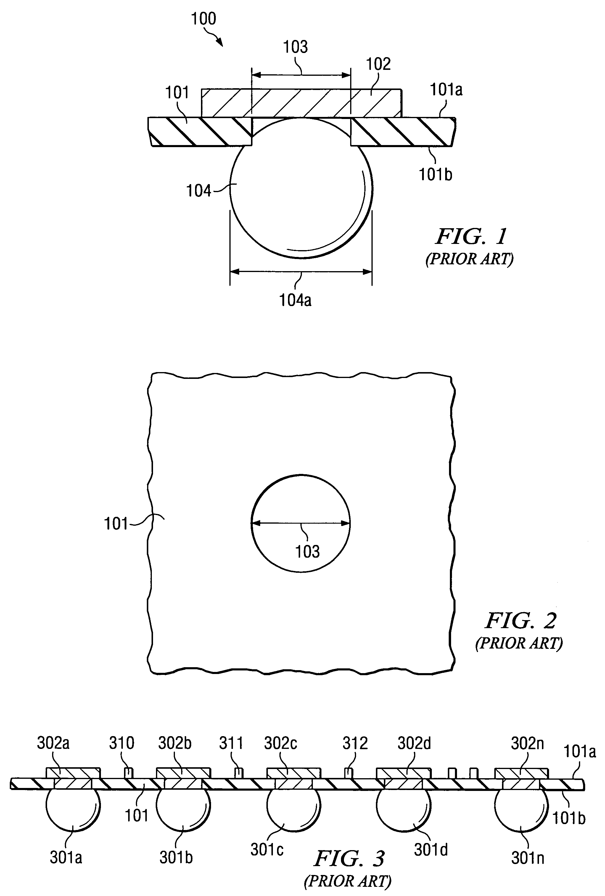
[0026]The impact of the present invention can be most easily appreciated by highlighting the shortcomings of the known technology. As a typical example of the known technology, the schematic cross section of FIG. 1 illustrates a solder-ball (solder bump) connection generally designated 100. In this connection, a substrate 101 with first surface 101a and second surface 101b has a metal layer on first surface 101a. The patterned portion 102 of this metal layer is exposed by a substrate window of diameter 103. This exposed layer portion is contacted by a solder body (“ball”, bump) 104, shown in FIG. 1 after attachment but before reflow; layer portion 102 is thus referred to as “contact pad”.

[0027]The dimensions of opening 103 are related to the diameter 104a of the solder body and the need of creating a large enough interface between body 104 and metal 102 to insure a reliable solder joint. As a consequence of this reliability requirement, window 103 and thus layer portion 102 consume ...


PUM

PropertyMeasurementUnit
thicknessaaaaaaaaaa
thicknessaaaaaaaaaa
diameteraaaaaaaaaa

Abstract

Semiconductor chip (1101) of a ball grid array device (1100) is mounted onto tape substrate (1102) using attach adhesive (1103). The metal layer on the top surface of substrate (1102) uses between about 30% to 90% of its area for connecting lines (1104), and only the remainder for members / rings (1105) and terminals (1106). Routing of differential pair signals and large numbers of signals on a single layer tape package are feasible. This embodiment creates an inexpensive high performance tape ball grid array package for chip-scale devices. Terminals (1106) serve the connection (by bonding wires or reflow bumps) to the chip contact pads. Inserted in members / rings (1105) are the conductive pins (1107), which serve as anchors for the solder bodies / balls (1108). Pins (1107) are substantially insensitive to the thermomechanical stresses, which occur in device (1100) during assembly, testing and operation.

Description

FIELD OF THE INVENTION[0001]The present invention is related in general to the field of semiconductor devices and processes and more specifically to structure and assembly method of tape-based high-density routing ball grid array packages featuring high reliability.DESCRIPTION OF THE RELATED ART[0002]A popular family of the semiconductor ball grid array packages uses a flexible tape as substrate. On one side (typically the bottom side) of this tape is an array of solder balls / bumps assembled for the package connection to external parts, and on the opposite side (typically the top side) of the tape is the semiconductor chip attached. In standard technology, one metal layer on the chip side of the tape provides the routing lines, further the terminals for attaching the interconnecting members to the chip assembly pads, and finally the contact pads for attaching the solder balls. The latter pads are exposed by pre-punched holes in the tape so that the solder balls / bumps can be attached...

Claims


Application Information

Patent Timeline
Patent Type & Authority Patents(United States)
IPC IPC(8): H05K1/16
CPCH01L23/49816H01L24/32H05K3/3426H01L23/49827H01L2224/83385H01L2224/32225H01L2224/48091H01L2224/48227H01L2224/73265H01L2924/01029H01L2924/01046H01L2924/0105H01L2924/01079H01L2924/01082H01L2924/15311H01L2924/3025H05K2201/10303H05K2201/10704H05K2201/10984H01L24/48Y10T29/49147H01L2924/01033H01L2924/00014H01L2924/00H01L2924/00012H01L24/73H01L2924/14H01L2924/181H01L2224/48472Y02P70/50H01L2224/45099H01L2224/45015H01L2924/207
Inventor HOWARD, GREGORY E.KALIDAS, NAVINHUNDT, PAUL J.MORRISON, GARY P.
Owner TEXAS INSTR INC
Why Eureka
Try Eureka