Apparatus and method for wafer level fabrication of high value inductors on semiconductor integrated circuits

a technology of semiconductor integrated circuits and wafers, applied in the direction of process and machine control, semiconductor/solid-state device details, instruments, etc., can solve the problems of insufficient flux or energy of inductors, high cost, and use of off-chip inductors

Active Publication Date: 2008-12-23
NAT SEMICON CORP
View PDF11 Cites 26 Cited by
  • Summary
  • Abstract
  • Description
  • Claims
  • Application Information

AI Technical Summary

Benefits of technology

[0008]An apparatus and method for wafer level fabrication of high value inductors directly on top of semiconductor integrated circuits is disclosed. The integrated circuit includes a plurality of regulator circuits, each of the regulator circuits having an input node configured to receive a plurality of pulsed input signals having a predetermined duty cycle and a plurality of inductor windings associated with each of the plurality of regulator circuits respectively. The integrated circuit also includes a core array having a plurality of core elements. The plurality of core elements are positioned adjacent to and mag

Problems solved by technology

In many situations, however, on chip inductors do not generate enough flux or energy for a particular application.
There are a number of problems in using off-chip inductors.
Foremost, they tend to be expensive.
Providing an off-chip inductor can therefore be relatively expensive compared to the overall cost of

Method used


Image

  • Apparatus and method for wafer level fabrication of high value inductors on semiconductor integrated circuits
  • Apparatus and method for wafer level fabrication of high value inductors on semiconductor integrated circuits
  • Apparatus and method for wafer level fabrication of high value inductors on semiconductor integrated circuits

Examples


Embodiment Construction

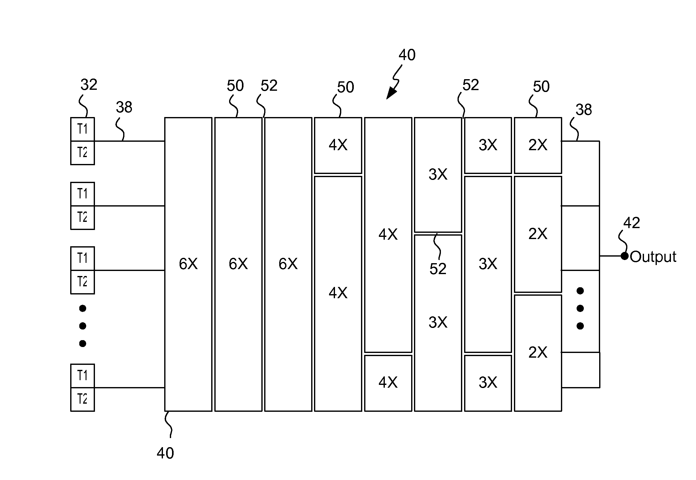
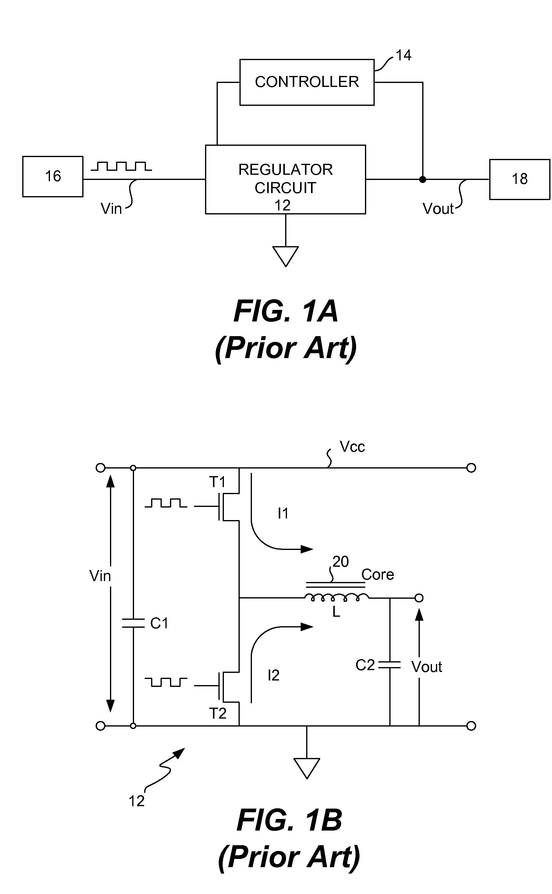
[0020]Referring to FIG. 1A, a block diagram of a common power regulator system is shown. The system 10 includes a regulator circuit 12 and a controller 14 coupled between a power supply 16 and a device 18, such as micro-controller, that requires a steady direct current (DC) voltage. The regulator circuit 12 includes an inductor (L) and a core (both not illustrated). The input voltage Vin is typically a pulsed input signal from the power supply 16 having a frequency (f) and an amplitude equal to Vin. With each positive and negative pulse transition, the inductor is cyclically energized and then de-energized, causing the flux in the core to increase and then decrease respectively. The output Vout of the regulator circuit 12 is coupled to the device 18. Ideally, the output voltage is steadily maintained at the desired output voltage. If the output voltage strays, the controller 14 causes the frequency (i.e., sometimes referred to as the duty cycle) of the pulses of the input voltage Vi...


PUM

PropertyMeasurementUnit
Lengthaaaaaaaaaa
Compositionaaaaaaaaaa
Densityaaaaaaaaaa

Abstract

An apparatus and method for wafer level fabrication of high value inductors directly on top of semiconductor integrated circuits is disclosed. The integrated circuit includes a plurality of regulator circuits, each of the regulator circuits having an input node configured to receive a plurality of pulsed input signals having a predetermined duty cycle and a plurality of inductor windings associated with each of the plurality of regulator circuits respectively. The integrated circuit also includes a core array having a plurality of core elements. The plurality of core elements are positioned adjacent to and magnetically coupled with one or more of the plurality of inductor windings. An output node is electrically coupled to the plurality of inductor windings. The output signal at the output node is the sum of the instantaneous voltage on each of the inductor windings associated with the plurality of regulator circuits respectively. The integrated circuit also includes a phase control circuit coupled to the plurality of regulator circuits. The phase control circuit controls the phase of the plurality of pulsed input signals received at the plurality of the regulator circuits to control the output signal at the output node.

Description

BACKGROUND[0001]1. Field of the Invention[0002]The present invention relates to wafer level fabrication of high value inductors on semiconductor integrated circuits, and more particularly, to the optimization of power inductor arrays on integrated circuits for switching regulator applications.[0003]2. Background of the Invention[0004]Inductors are commonly used in the electronics industry for storing magnetic energy. Providing an electric current though a metal conductor, such as a metal plate or bar, typically creates an inductor. The current passing though the metal conductor creates a magnet field or flux around the conductor. The amount of inductance is measured in terms of Henries. In the semiconductor industry, it is known to form inductors on integrated circuits. The inductors are typically created by fabricating what is commonly called an “air coil” inductor on the chip. The air coil inductor is usually either aluminum or some other metal patterned in a helical, toroidal or ...

Claims


Application Information

Patent Timeline
IPC IPC(8): G05F1/59G05F1/618
CPCH01L23/5227H01F17/0006H01F41/046Y10T29/49071Y10T29/49073Y10T29/49075Y10T29/4902Y10T29/49124Y10T29/4913H01L2924/0002H01L2924/00
Inventor HOPPER, PETER J.JOHNSON, PETERSMEYS, PETERPAPOU, ANDREI
Owner NAT SEMICON CORP
Why Eureka
Try Eureka