Storage device and semiconductor device

a storage device and semiconductor technology, applied in static storage, digital storage, instruments, etc., can solve the problems of slow reading speed, information disappearance, non-destructive readout, etc., and achieve the effect of stable recording and shortening the time taken for recording information

Active Publication Date: 2008-12-30
SONY SEMICON SOLUTIONS CORP
View PDF16 Cites 21 Cited by
  • Summary
  • Abstract
  • Description
  • Claims
  • Application Information

AI Technical Summary

Benefits of technology

[0029]The present invention has been made in view of the above, and it is desirable to provide a storage device and a semiconductor device that can perform stable recording, shorten a time taken for recording information, and erase a storage element after writing.
[0035]The storage device and the semiconductor device according to the embodiments of the present invention as described above can perform stable recording, shorten a time taken for recording information, and erase the storage element after writing.

Problems solved by technology

However, since DRAMs are volatile memories whose information disappears when power is turned off.
However, in the case of FeRAM, currently it is difficult to perform a nondestructive readout, and since a destructive readout is performed, a reading speed is slow.
Moreover, the number of times of polarization inversion by reading or recording is limited, and thus there is a limitation to the number of times that FeRAM can be rewritten.
Therefore a large amount of current may be required when recording is performed.
However, the phase change memory causes switching according to a temperature, and is therefore sensitive to a change in ambient temperature.
Thus, the PMC may not endure a high temperature in a process of actually producing a memory element, for example a process of forming a CVD insulating film, a protective film or the like.
Therefore problems occur in that, for example, a heat treatment at approximately 600° C. has to be performed, it is very difficult to manufacture a single crystal of the proposed materials, and miniaturization is difficult due to effects of a grain boundary when a polycrystal is used.
It is therefore difficult to perform the recording stably.
Thus, a long time is taken for recording, and it is difficult to perform overwriting of data or the like at a high speed, for example.

Method used


Image

  • Storage device and semiconductor device
  • Storage device and semiconductor device
  • Storage device and semiconductor device

Examples


Embodiment Construction

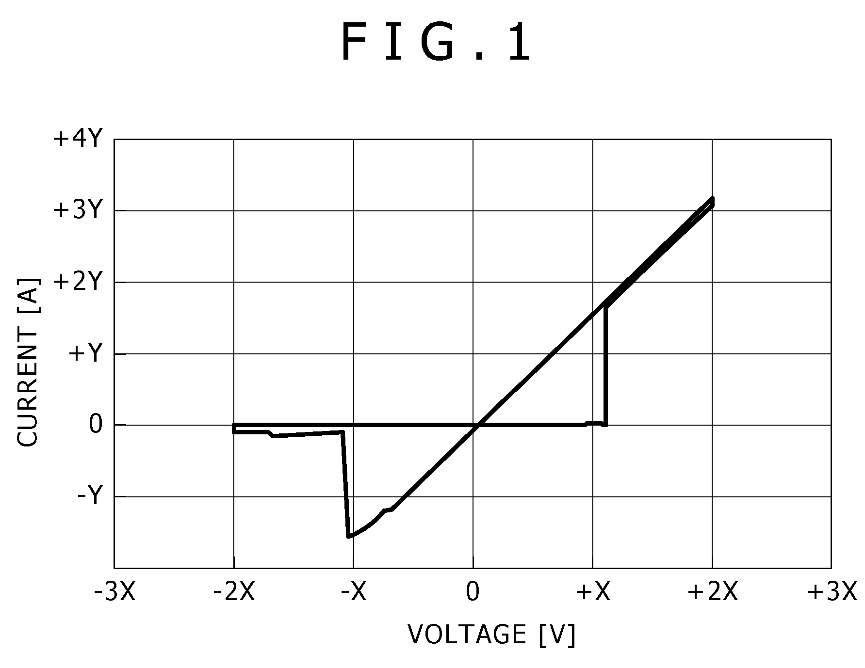
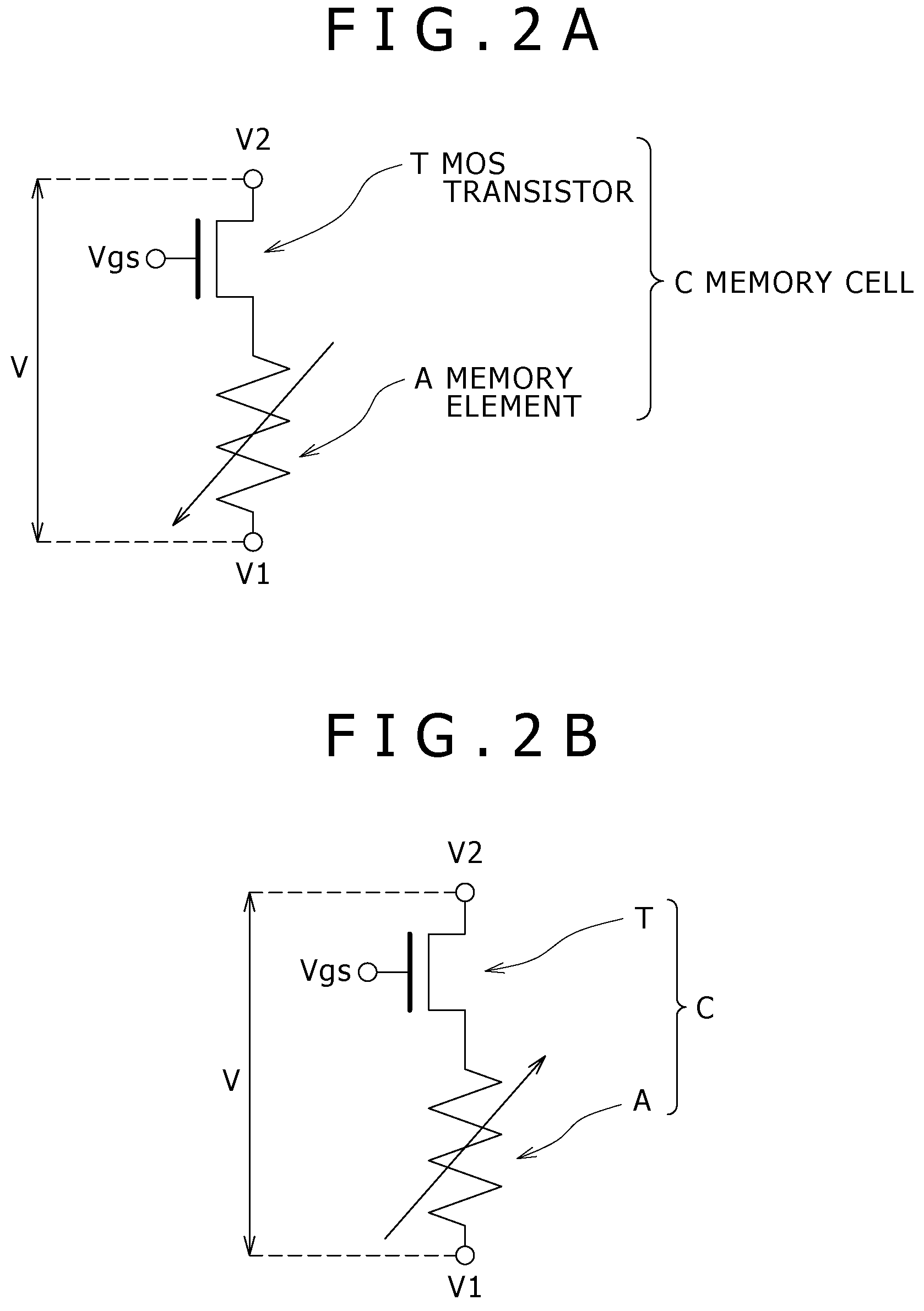
[0054]A preferred embodiment of the present invention will hereinafter be described with reference to the drawings, for understanding of the present invention. Incidentally, in the present embodiment, a storage device is formed by using a resistance change type storage element (hereinafter referred to as a memory element) in a memory cell, and the memory element in this case is an example of a storage element.

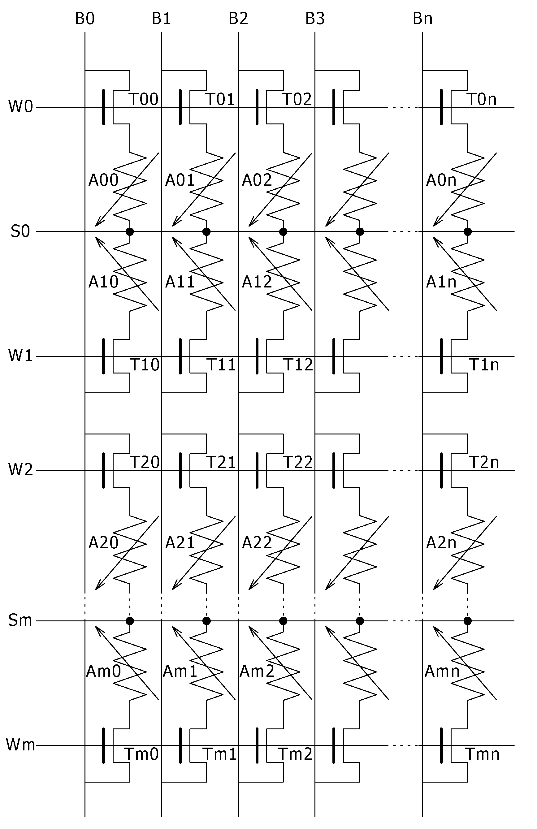
[0055]FIG. 1 is a graph showing current-voltage (I-V) changes of a memory element used in an example of a storage device to which the present invention is applied.

[0056]Incidentally, the memory element having the I-V characteristics as shown in FIG. 1 includes a storage element formed by interposing a storage layer between a first electrode and a second electrode, for example (between a lower electrode and an upper electrode, for example), the storage layer being composed of an amorphous thin film such as a rare-earth oxide film, for example.

[0057]This memory element in an init...


PUM


Abstract

A storage device includes a memory cell having a storage element having a characteristic of changing from a state of a high resistance value to a state of a low resistance value by being supplied with a voltage equal to or higher than a first threshold voltage, and changing from a state of a low resistance value to a state of a high resistance value by being supplied with a voltage equal to or higher than a second threshold voltage different in polarity from the first threshold voltage, and a circuit element connected in series with the storage element, wherein letting R be a resistance value of the storage element after writing, V be the second threshold voltage, and I be a current that can be passed through the storage element at a time of erasure, R≧V / I.

Description

CROSS REFERENCES TO RELATED APPLICATIONS[0001]The present invention contains subject matter related to Japanese Patent Application JP 2005-263513 filed with the Japanese Patent Office on Sep. 12, 2005, the entire contents of which being incorporated herein by reference.BACKGROUND OF THE INVENTION[0002]1. Filed of the Invention[0003]The present invention relates to a storage device and a semiconductor device, and particularly to a storage device and a semiconductor device formed with a memory cell using a storage element that stores and retains information by a state of an electric resistance.[0004]2. Description of the Related Art[0005]In information devices such as computers and the like, a DRAM (Dynamic Random Access Memory) operating at a high speed and having a high density is widely used as a random access memory.[0006]However, since DRAMs are volatile memories whose information disappears when power is turned off. Therefore nonvolatile memories whose information does not disap...

Claims


Application Information

Patent Timeline
Patent Type & Authority Patents(United States)
IPC IPC(8): G11C11/00
CPCG11C13/0007G11C13/0011G11C13/0069G11C2013/009G11C2213/31G11C2213/79G11C5/063
Inventor NAKASHIMA, CHIEKOHACHINO, HIDENARINAGAO, HAJIMEOKAZAKI, NOBUMICHI
Owner SONY SEMICON SOLUTIONS CORP
Why Eureka
Try Eureka