

Optical modulator
- Summary
- Abstract
- Description
- Claims
- Application Information
AI Technical Summary
Benefits of technology
Problems solved by technology
Method used
Image

Examples
first embodiment
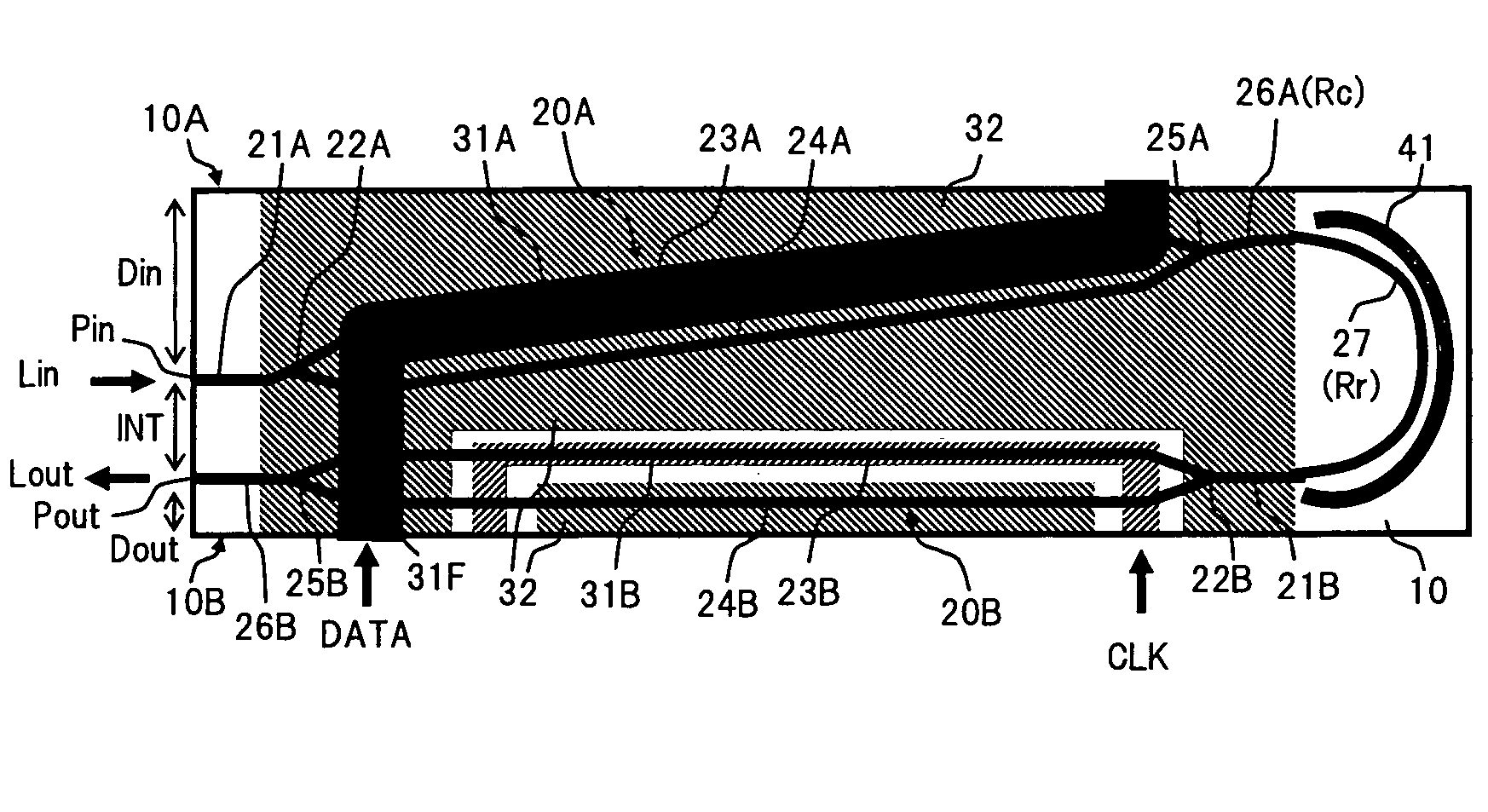
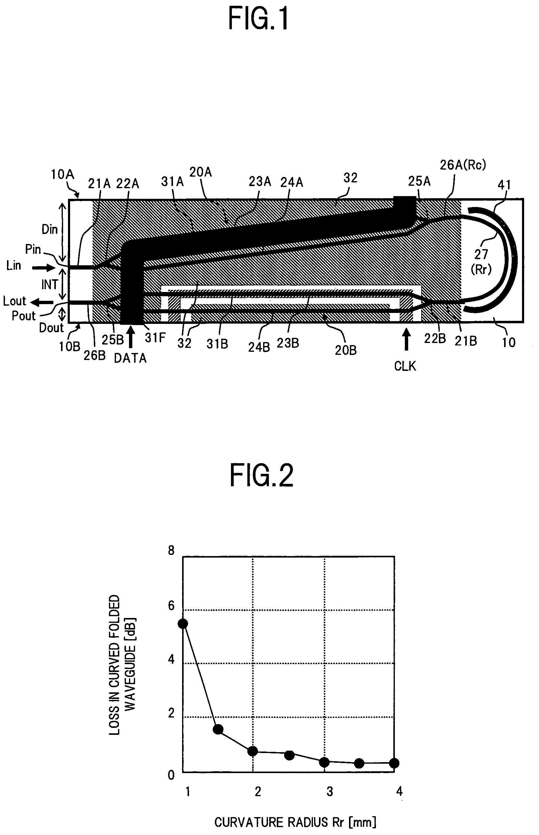
[0030]FIG. 1 is a plan view showing the configuration of an optical modulator according to the present invention.
[0031]In FIG. 1, the optical modulator according to the embodiment includes, for example, a substrate (chip) 10 having an electrooptic effect, two Mach Zehnder (MZ) type optical waveguide units 20A and 20B formed on the substrate 10, signal electrodes 31A and 31B formed on a surface of the substrate 10 in association with the Mach Zehnder (MZ) type optical waveguide units 20A and 20B, and a ground electrode 32.
[0032]As the substrate 10, for example, a crystal substrate consisting of z-cut lithium niobate (LiNbO3) or lithium tantalate (LiTaO2) is used. The substrate used in the present invention is not limited to the example described above. The present invention is effective for a known substrate material having an electrooptic effect.
[0033]The MZ type optical waveguide units 20A and 20B have, for example, input waveguides 21A and 21B, branch portions 22A and 22B, branch ...
second embodiment
[0044]the present invention will be described below.
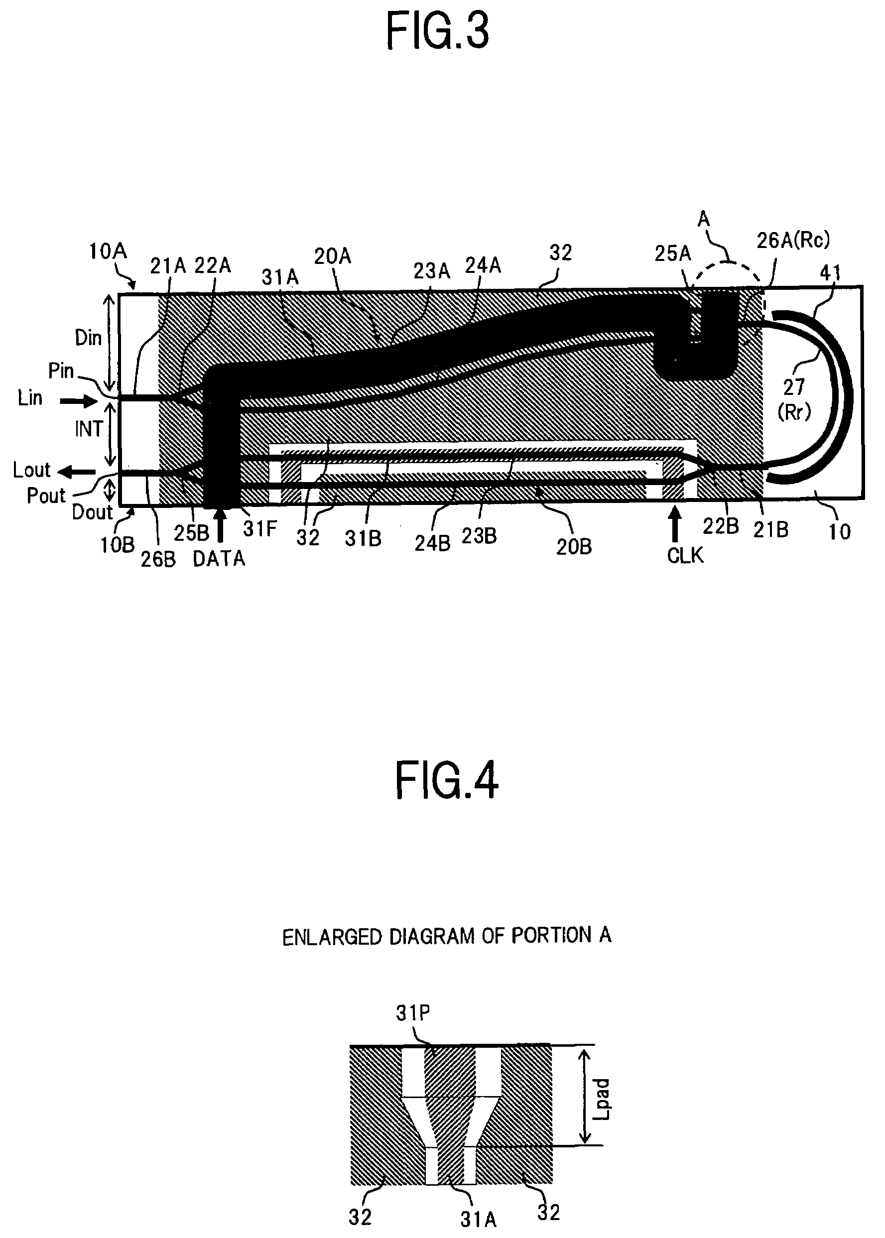
[0045]FIG. 3 is a plan view showing a configuration of an optical modulator according to the second embodiment of the present invention.
[0046]In FIG. 3, the optical modulator according to the embodiment is obtained such that, in the configuration of the first embodiment shown in FIG. 1, the shape of the MZ type optical waveguide unit 20A on the input side is changed into an S shape, and the pattern of the terminal portion of the signal electrode 31A located near the side surface 10A of the substrate 10 is changed. Since the configurations other than the shape of the MZ type optical waveguide unit 20A and the pattern of the signal electrode 31A are the same as those in the first embodiment, a description thereof will be omitted.
[0047]The first embodiment shows an example in which the output waveguide 26A of the MZ type optical waveguide unit 20A is curved at the curvature radius Rc larger than the curvature radius Rr of the curved f...
third embodiment
[0051]the present invention will be described below.
[0052]FIG. 5 is a plan view showing a configuration of an optical modulator according to the third embodiment of the present invention.
[0053]In FIG. 5, the optical modulator according to this embodiment is obtained such that, in the configuration of the second embodiment shown in FIG. 3, the shape of the substrate 10 is changed into a trapezoidal shape by using a shape designed to have a distance between the two MZ type optical waveguide units 20A and 20B which is smaller on an input / output port side than on a curved folded waveguide 27 side. More specifically, the substrate 10 is preferably cut to satisfy the following conditions. That is, opposite end faces 10C and 10D of the substrate 10 located on the light and left in FIG. 5 are almost parallel to each other, and an angle between the opposite end faces 10C and 10D and the side surface 10A located on the upper side in FIG. 5 is almost 90°.
[0054]When the substrate 10 is formed i...
PUM
 Abstract
Description
Claims
Application Information