Method of creating predictive model, method of managing process steps, method of manufacturing semiconductor device, method of manufacturing photo mask, and computer program product

a predictive model and process step technology, applied in the field of creating predictive models, can solve the problems of difficult to set a target of an allowable fluctuation amount of a process, difficult to manage the steps of manufacturing a semiconductor from a viewpoint of ppe, and difficult to verify the precision of the cd value obtained by extrapolation

Active Publication Date: 2009-01-06
KIOXIA CORP
View PDF5 Cites 11 Cited by
  • Summary
  • Abstract
  • Description
  • Claims
  • Application Information

AI Technical Summary

Problems solved by technology

However, it is difficult to verify precision of the CD value obtained by the extrapolation.
Moreover, as a result of the drop of the prediction precision in the actually required pitch, it is difficult to set a target of an allowable fluctuation amount of a process in a case where the process is managed in consideration of the PPE in each step.
That is, it is difficult to manage steps of manufacturing a semiconductor from a viewpoint of the PPE.

Method used


Image

  • Method of creating predictive model, method of managing process steps, method of manufacturing semiconductor device, method of manufacturing photo mask, and computer program product
  • Method of creating predictive model, method of managing process steps, method of manufacturing semiconductor device, method of manufacturing photo mask, and computer program product
  • Method of creating predictive model, method of managing process steps, method of manufacturing semiconductor device, method of manufacturing photo mask, and computer program product

Examples


first embodiment

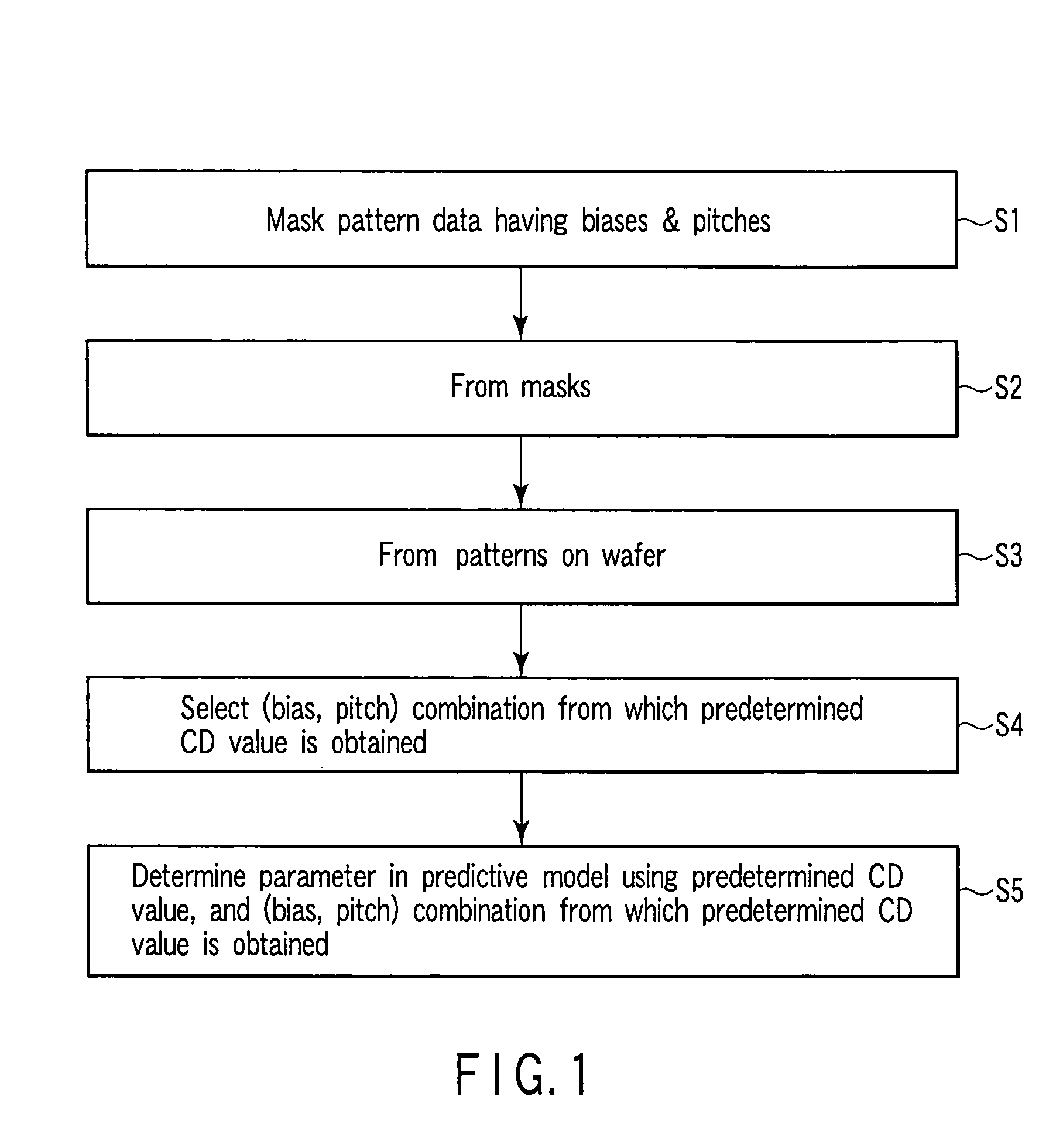
[0046]FIG. 1 is a flowchart showing a method of creating a process proximity effect predictive model (hereinafter referred to simply as the predictive model) according to a first embodiment of the present invention. Here, a method of creating the predictive model will be described which is of such a type that a finally obtained dimension of a pattern on a wafer is directly predicted from mask drawing data.

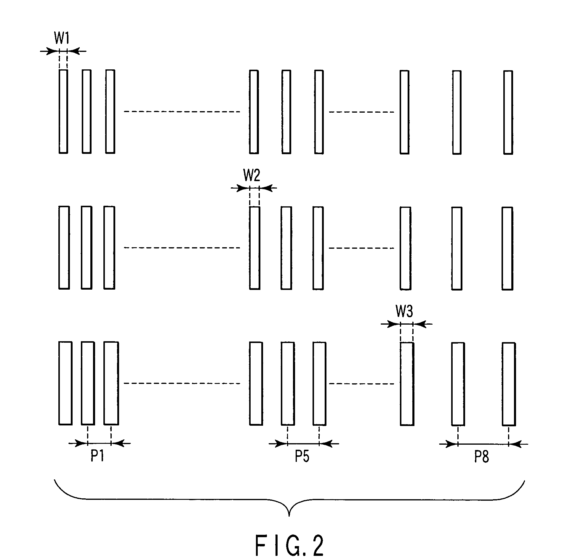
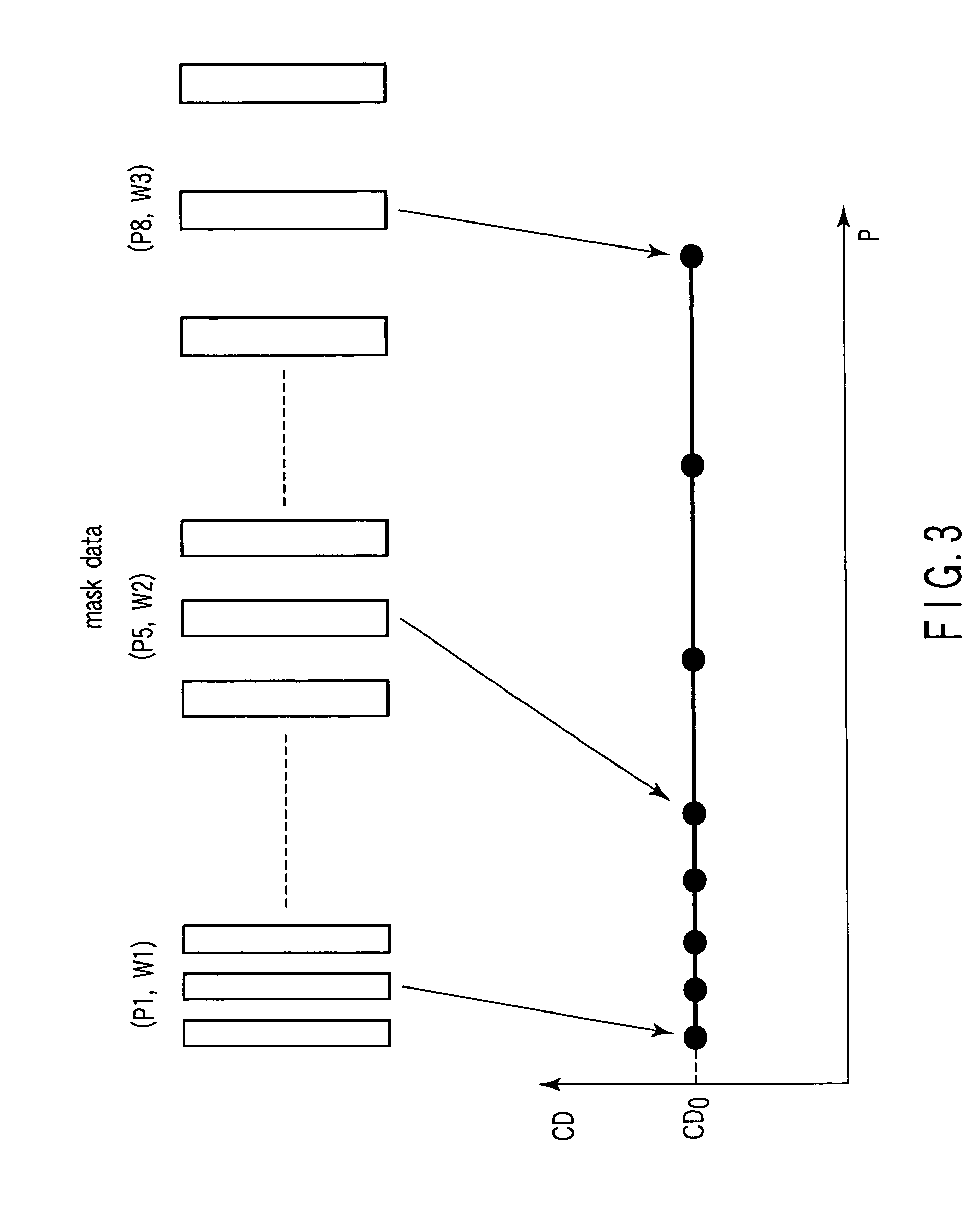
[0047]First, the mask drawing data (mask pattern data) is prepared corresponding to a pattern group for modeling which comprises a plurality of line & space patterns obtained by changing line widths (biases) of line patterns and pitches of the line & space patterns with respect to a line & space patterns which comprises repetition line patterns (step S1).

[0048]Here, the line & space pattern group shown in FIG. 2 are used as the pattern group for modeling. There are three types of line widths (biases) W1 to W3. There are eight types of pitches P1 to P8. Therefore, the mask drawing d...

second embodiment

[0083]FIGS. 8A to 8C are explanatory views showing a method of managing a semiconductor manufacturing step according to the second embodiment of the present invention.

[0084]In FIGS. 8A to 8C, the ordinate shows a dimension difference (ΔCD) between the present step and the previous step. Concretely, the ordinate ofFIG. 8A shows CD of a photo mask (present step)-CD of the mask drawing data (one step before), the ordinate of FIG. 8B shows CD of a resist (present step)-CD of the photo mask (one step before), and the ordinate of FIG. 8C shows CD of a wafer pattern (present step)-CD of the resist (one step before). The abscissa shows a pattern environment (e.g., the pitch of the line & space pattern of the first embodiment) P.

[0085]One-dot chain lines in FIGS. 8A to 8C shows the pattern environment P in which a predetermined dimension is obtained after a processing step and a target value of ΔCD corresponding to the environment. Instead of the target value of ΔCD, a dimension difference b...

third embodiment

[0153]The third embodiment of the present invention will be described hereinafter. As described in the present specification, as the method of setting the control width with respect to the target dimension for each of the steps (the step of forming the mask drawing data, the step of manufacturing the photo mask, the lithography step, the processing step) of the manufacturing process of a semiconductor device), the following methods (1) and (2) have been described:

[0154](1) the method of equally dividing the control width with respect to the average value or the standard deviation value of the residual from the target line width in all the patterns; and

[0155](2) the method of converting the dimension fluctuation attributed to each step into the final finally obtained dimension fluctuation in consideration of the dimension fluctuation sensitivity between the steps to set the control width of each step.

[0156]In the present embodiment, a method of managing the steps in consideration of ...


PUM

PropertyMeasurementUnit
widthaaaaaaaaaa
dimensionaaaaaaaaaa
widthaaaaaaaaaa

Abstract

A method of creating a predictive model of a process proximity effect comprises: preparing a predictive model of a process proximity effect including a non-determined parameter; and determining the non-determined parameter, the method comprises: preparing a pattern group for modeling, the pattern group comprising a plurality of repetition patterns, the plurality of repetition patterns being obtained by changing a first and second dimensions of a repetition pattern which repeats a basic pattern, the first dimension defining the basic pattern, and the second dimension defining repetition of the basic pattern; selecting a predetermined repetition pattern from the pattern group for modeling, the basic pattern of the predetermined repetition pattern corresponding to a pattern which is to be formed on a wafer and has a predetermined dimension; and determining the non-determined parameter in the predictive model based on the predetermined repetition pattern and the pattern having the predetermined dimension.

Description

CROSS-REFERENCE TO RELATED APPLICATIONS[0001]This application is based upon and claims the benefit of priority from the prior Japan Patent Applications No. 2003-209310, Aug. 28, 2003, and Japan Patent Applications No. 2004-240883, Aug. 20, 2004, the entire contents of both of which are incorporated herein by reference.BACKGROUND OF THE INVENTION[0002]1. Field of the Invention[0003]The present invention relates to a method of creating a predictive model for use in process proximity effect correction, a method of managing process steps, a method of manufacturing a semiconductor device, a method of manufacturing a photo mask, and a computer program product.[0004]2. Description of the Related Art[0005]In recent years, with miniaturization of LSI, a pattern on a photo mask (mask pattern), having a dimension below 1 μm, has been required. By the miniaturization of the mask pattern, phenomena in which a resist pattern cannot be formed as designed on a wafer in a lithography step, that is, ...

Claims


Application Information

Patent Timeline
Patent Type & Authority Patents(United States)
IPC IPC(8): G03F9/00G03F1/36G03F1/68G06F17/50H01L21/02H01L21/027
CPCG03F1/144G06F17/5068G03F1/36G06F30/39G03F7/70441G03F7/705
Inventor TANAKA, SATOSHIINOUE, SOICHIHASHIMOTO, KOJIHASEBE, SHIGERU
Owner KIOXIA CORP
Why Eureka
Try Eureka