Silicon carrier including an integrated heater for die rework and wafer probe

Active Publication Date: 2009-01-06
IBM CORP
View PDF10 Cites 32 Cited by
  • Summary
  • Abstract
  • Description
  • Claims
  • Application Information

AI Technical Summary

Benefits of technology

[0007]The shortcomings of the prior art are overcome and additional advantages are provided through the provision of a silicon carrier package constructed in accordance with an exemplary embodiment of the present invention. The silicon carrier package includes a multi-layer member having at least a first layer and a second layer. A first electronic component includes a plurality of connector members that establish a first bond electrically interconnecting the first electronic component to the multi-layer member. A second electronic compon

Problems solved by technology

At present, removal of a single defective electronic component or chip from a multi-chip silicon carrier or module (MCM) is a challenge.
That is, often times removing one chip will also melt adjacent solder joints and degrade connections for adjacent components.
Other processes currently in use for chip removal, such as various chemical removal methods, are cumbersome.
Similar difficulties occur when replacing defective chips with good chips.
However, it is often the case that in spite of tests done with TCA, one or more device die components fail fully functional tests performed after assembly of the chip module.
However, as noted above, a major drawback of this method is that all chip interconnections in the module are melted thereby subjecting all chips to a reflow of solder.
Another problem encountered during die rework co

Method used


Image

  • Silicon carrier including an integrated heater for die rework and wafer probe
  • Silicon carrier including an integrated heater for die rework and wafer probe
  • Silicon carrier including an integrated heater for die rework and wafer probe

Examples


Example

[0013]The detailed description explains the exemplary embodiments of the invention, together with advantages and features, by way of example with reference to the drawings.

DETAILED DESCRIPTION OF THE INVENTION

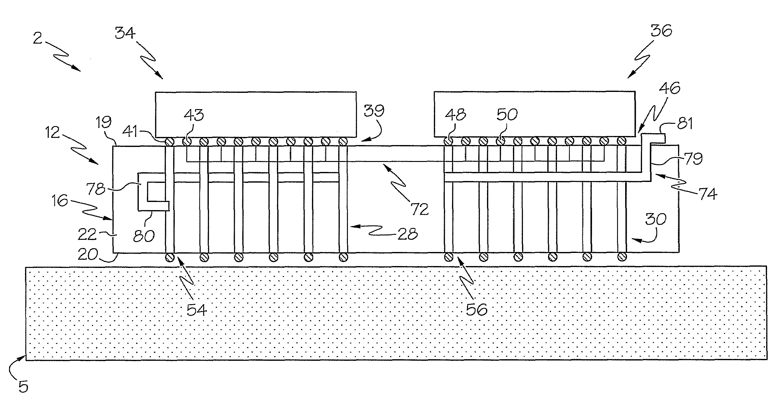
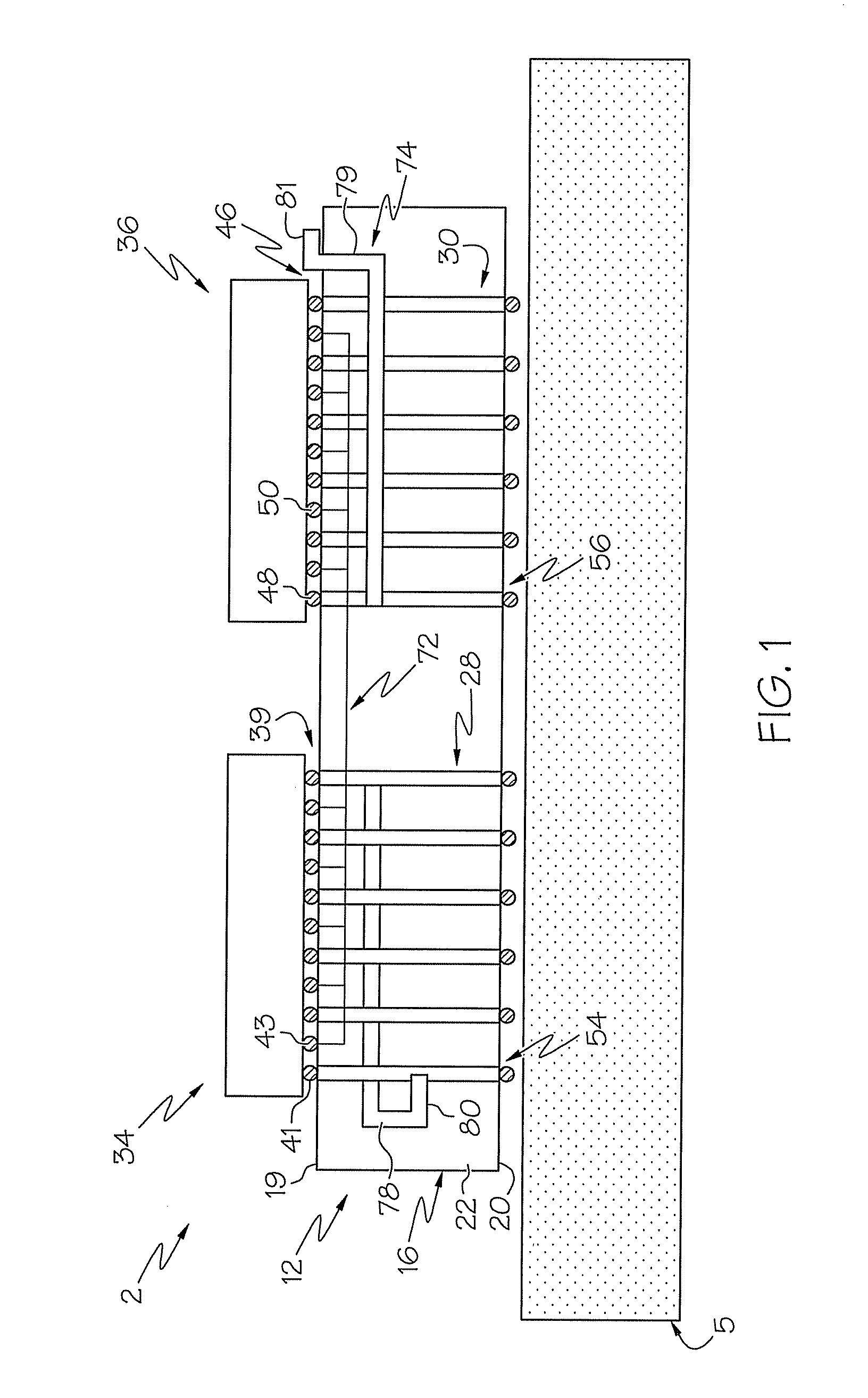
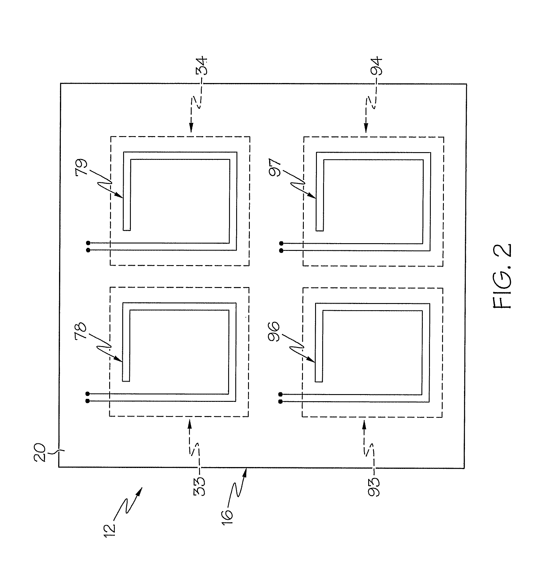
[0014]With initial reference to FIG. 1, a silicon carrier or interposer package in the form of a multi-chip module (MCM) is indicated generally at 2. Multi-chip module 2 is mounted to a substrate 5 and includes a silicon interposer member 12. Interposer member 12 includes a main body portion 16 having a first surface 19, a second surface 20, and an intermediate portion 22. Interposer member 12 includes a first plurality of vias, indicated generally at 28 that extend between first and second surfaces 19 and 20. Interposer member 12 is also shown to include a second plurality of vias, indicated generally at 30, that extend between first and second surfaces 19 and 20 and which are laterally offset from the first plurality of vias 28.

[0015]A first electronic component 34, shown in ...


PUM


Abstract

A silicon carrier package includes a multi-layer member having at least a first layer and a second layer. A first electronic component includes a plurality of connector members that establish a first bond electrically interconnecting the first electronic component to the multi-layer member. A second electronic component includes a plurality of connector members that establish a second bond electrically interconnecting the second electronic component to the multi-layer member. At least one heating element is integrated into one of the first and second layers of the multi-layer member. The at least one heating element is selectively activated to loosen only one of the first and second bonds to facilitate removal of only one of the first and second electronic components from the multi-layer member. The other of the first and second bonds remains intact.

Description

STATEMENT OF GOVERNMENT INTEREST[0001]This invention was made with Government support under Contract No. NBCH3039004, awarded by the US Defense Advanced Research Projects Agency (DARPA). The Government has certain rights in this invention.BACKGROUND OF THE INVENTIONField of the Invention[0002]This invention relates to the art of electronics and, more particularly, to a silicon carrier having an integrated heater to facilitate removal, attachment and testing of electronic components.DESCRIPTION OF BACKGROUND[0003]At present, removal of a single defective electronic component or chip from a multi-chip silicon carrier or module (MCM) is a challenge. That is, providing enough heat to melt solder joints that hold the defective chip to the MCM creates multiple solder reflows that are added to a process thermal budget. That is, often times removing one chip will also melt adjacent solder joints and degrade connections for adjacent components. By degrading adjacent connections, an overall e...

Claims


Application Information

Patent Timeline
IPC IPC(8): H05K1/11
CPCH01L23/147H01L23/345H01L24/98H01L25/0655H01L23/5384H01L24/81Y10T29/4913H01L2224/81234H01L2224/81815H01L2924/01082H01L2924/09701H01L2924/01033H01L2224/16235H01L2924/14H01L2924/00
Inventor DANG, BINGWRIGHT, STEVEN L.
Owner IBM CORP
Why Eureka
Try Eureka