Dry-etching method

Inactive Publication Date: 2009-01-13
TOKYO ELECTRON LTD
View PDF14 Cites 3 Cited by
  • Summary
  • Abstract
  • Description
  • Claims
  • Application Information

AI Technical Summary

Benefits of technology

[0008]It is, therefore, an object of the present invention to provide a dry etching method capable of increasing a selectivity of a silicon-containing conductive film against a silicon oxide film such that only desired silicon-containing cond

Problems solved by technology

However, circuit patterns of semiconductor

Method used


Image

  • Dry-etching method
  • Dry-etching method
  • Dry-etching method

Examples


Example

[0024]A preferred embodiment of the present invention will now be described hereinafter with reference to the accompanying drawings.

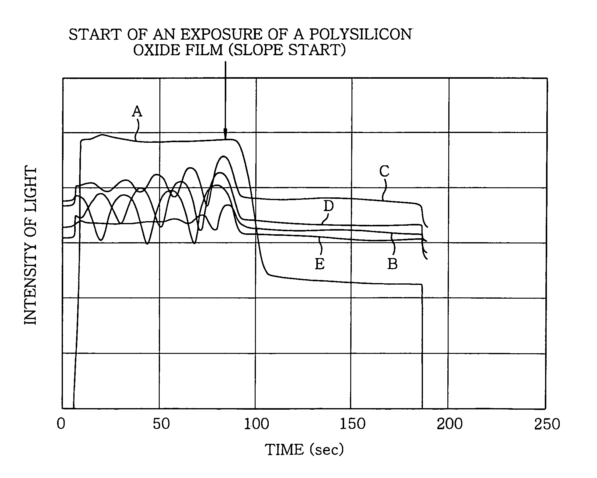
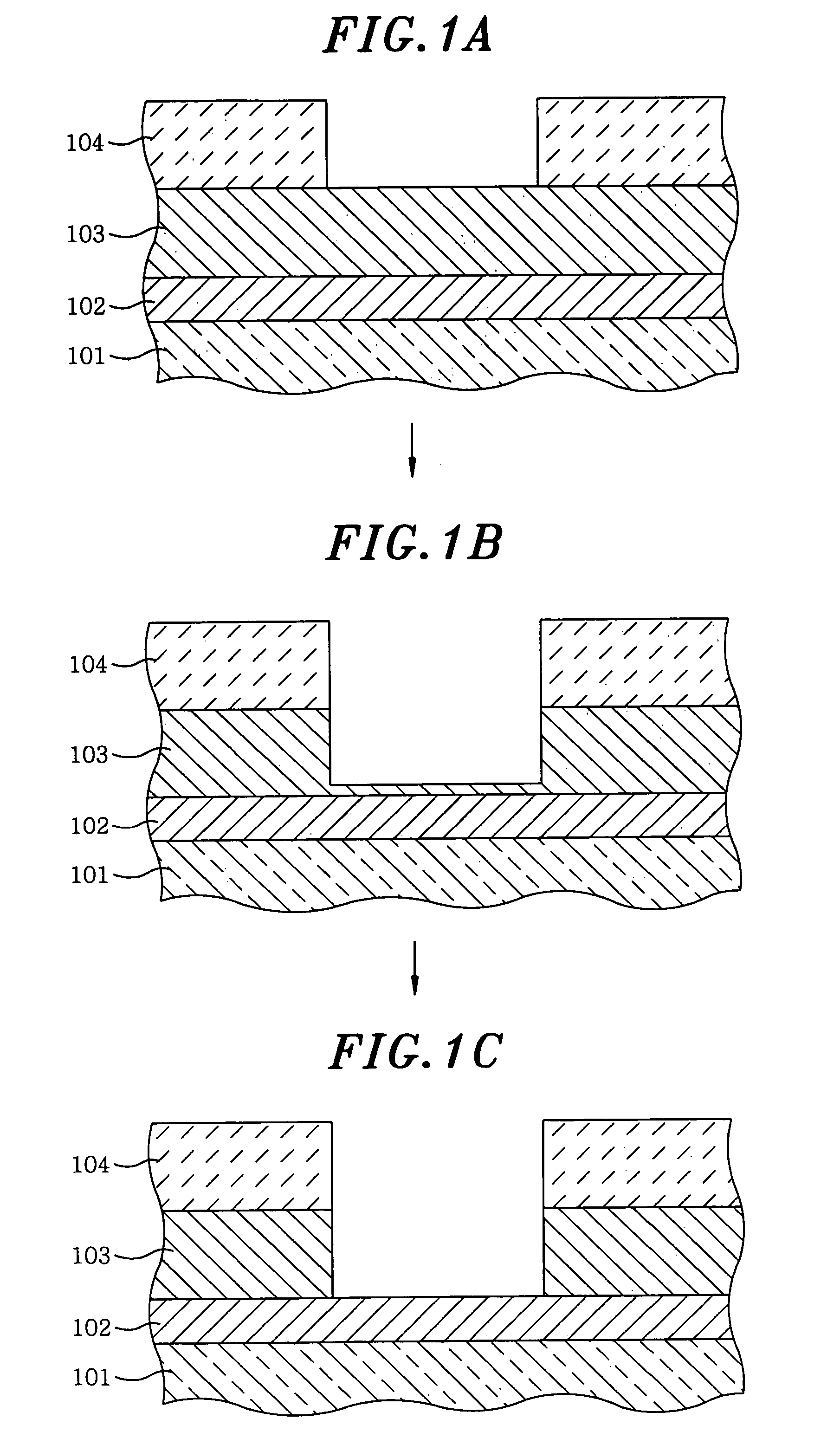
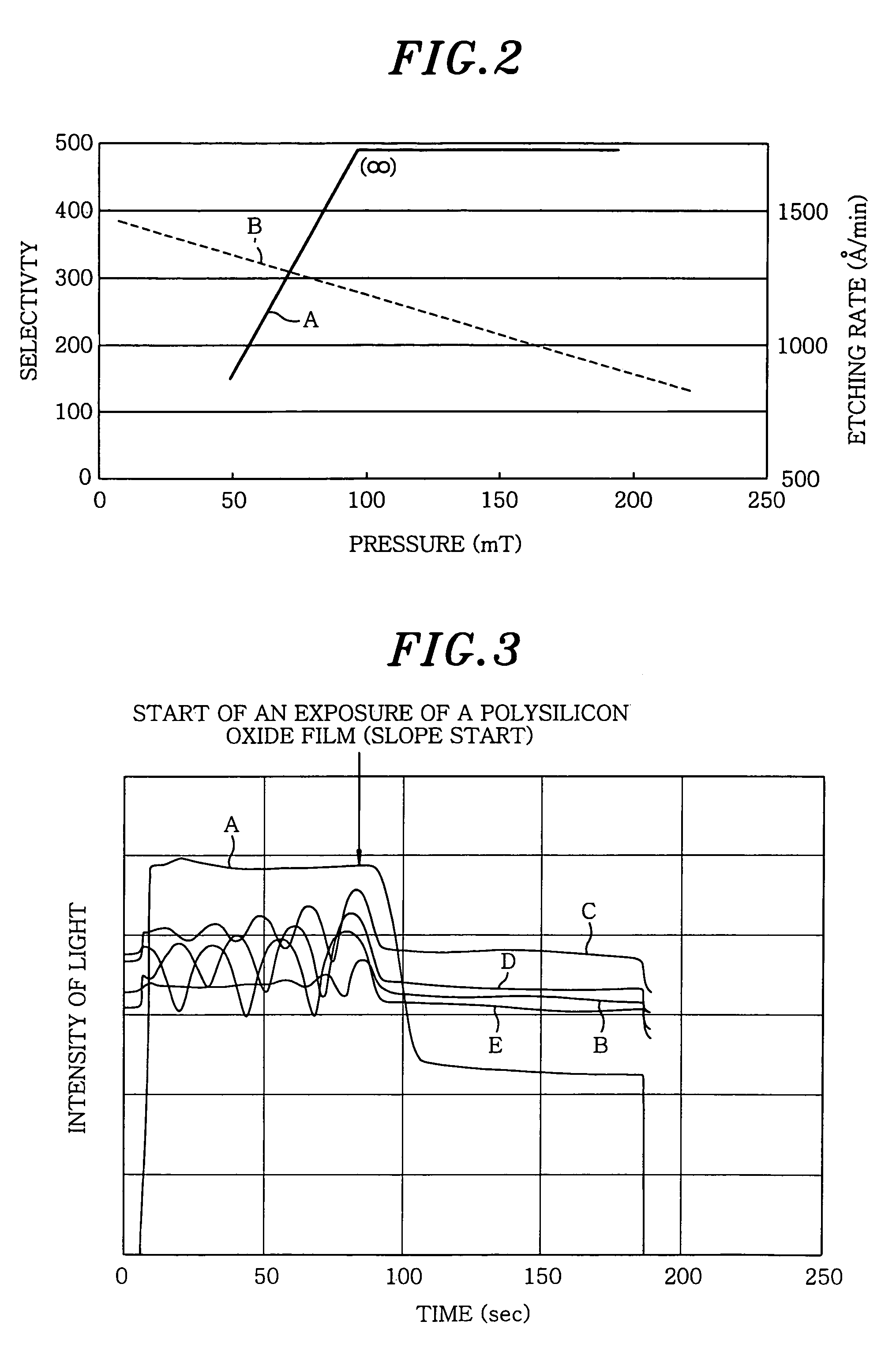
[0025]Referring to FIGS. 1A to 1C, there are illustrated partially enlarged schematic longitudinal cross sectional views of a semiconductor wafer (silicon substrate) for explaining the preferred embodiment of the present invention.

[0026]As shown in FIG. 1A, formed on the semiconductor wafer (silicon substrate) 101 are a silicon oxide film layer 102 forming an insulating layer and a silicon-containing conductive film layer 103 forming a conductor layer (e.g., a polys ilicon layer, a silicide layer, or a polysilicon layer and a silicide layer disposed thereon).

[0027]Further, formed on the silicon-containing conductive film layer 103 is a mask layer 104 made of a photoresist or a so-called hard mask (silicon nitride, for example) and having a predetermined pattern.

[0028]In this preferred embodiment, the silicon-containing conductive film layer 103 is etche...


PUM


Abstract

A main etching step is effected in a state shown in FIG. 1A under a first pressure using a gas containing at least HBr, e.g., a mixture gas of HBr and Cl2 as an etching gas. The main etching is ended before a silicon oxide film 102, as shown in FIG. 1B, is exposed. An over-etching process is effected under a second pressure higher than the first pressure using a gas containing at least HBr, e.g., an HBr single gas so as to completely expose the silicon oxide film 102 as shown in FIG. 1C. In such a way, the selectivity of a silicon-containing conductive layer with respect to the silicon oxide film is improved compared to conventional methods. Without etching the silicon oxide film layer, which is an underlying layer, and without marring the shape of the silicon-containing conductive film layer formed by etching, only the desired silicon-containing conductive film layer is removed by etching reliably.

Description

FIELD OF THE INVENTION[0001]The present invention relates to a dry etching method for use in manufacturing a semiconductor device; and, more particularly, to a dry etching method for etching a silicon-containing conductive film layer formed on a silicon oxide film layer.BACKGROUND OF THE INVENTION[0002]To conventionally fabricate, e.g., a gate structure in a manufacturing process of a semiconductor device, a conductor layer [a silicon-containing conductive film layer (e.g., a polysilicon layer, a silicide layer, or a polysilicon layer and a silicide layer deposited thereon)] is formed on an insulating layer of a silicon oxide film layer. Thereafter, the conductor layer is etched into a predetermined pattern through a mask layer formed thereon until the underlying silicon oxide film layer is exposed.[0003]Conventionally, a plasma etching has been widely employed for etching such a silicon-containing conductive film layer formed on the silicon oxide film layer.[0004]When plasma etchin...

Claims


Application Information

Patent Timeline
IPC IPC(8): H01L21/302H01L21/3213
CPCH01J37/32935H01L21/32137H01L21/3065
Inventor IIJIMA, ETSUOYAMADA, NORIKAZU
Owner TOKYO ELECTRON LTD
Why Eureka
Try Eureka