

Process for producing GaN substrate
a technology of gan substrate and gan pore, which is applied in the direction of crystal growth process, polycrystalline material growth, after-treatment details, etc., can solve the problems of low yield, inability to achieve the growth of large crystal substrates of 1 inch or more in the future, and cannot be technically established
- Summary
- Abstract
- Description
- Claims
- Application Information
AI Technical Summary
Benefits of technology
Problems solved by technology
Method used
Image

Examples
Embodiment Construction
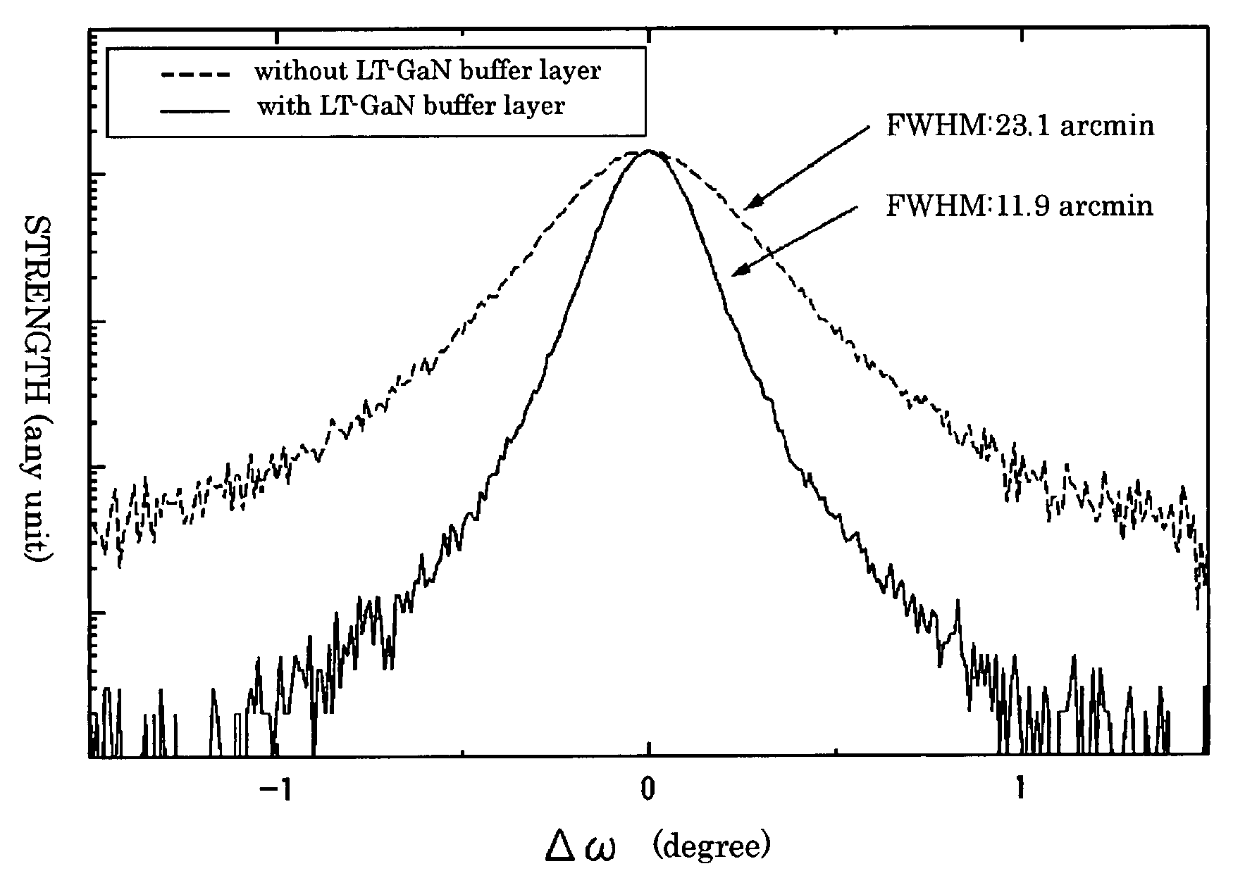
[0025]In the present invention, MgO buffer is grown on a high-quality substrate, a ZnO single crystal film is formed thereon, and a GaN single crystal film is further grown thereon. At this time, the GaN single crystal film is grown while performing polarity control, and ZnO is melted, whereby a GaN single crystal substrate is separated.
[0026]According to this, a high-quality GaN single crystal of Ga polarity can be obtained.
[0027]A preferred embodiment of the present invention will be described in reference to the accompanying drawings.
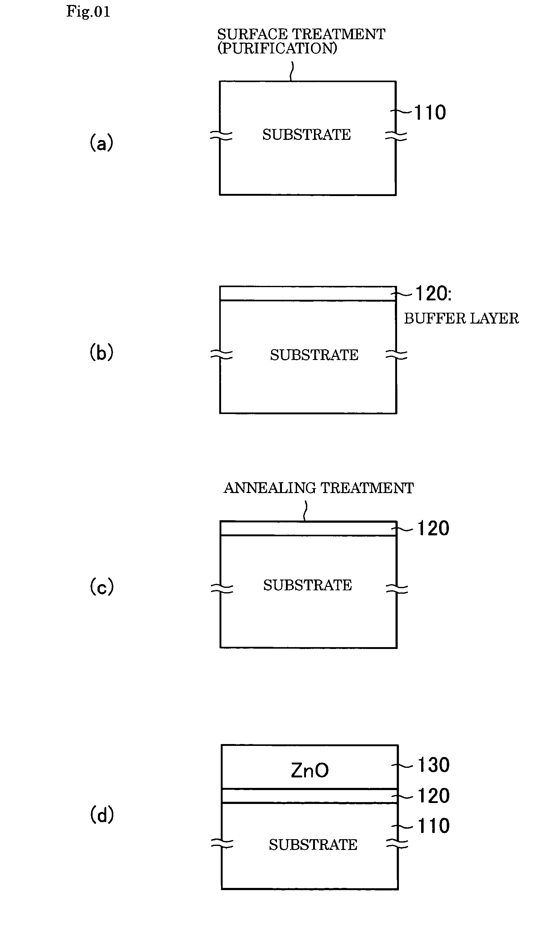
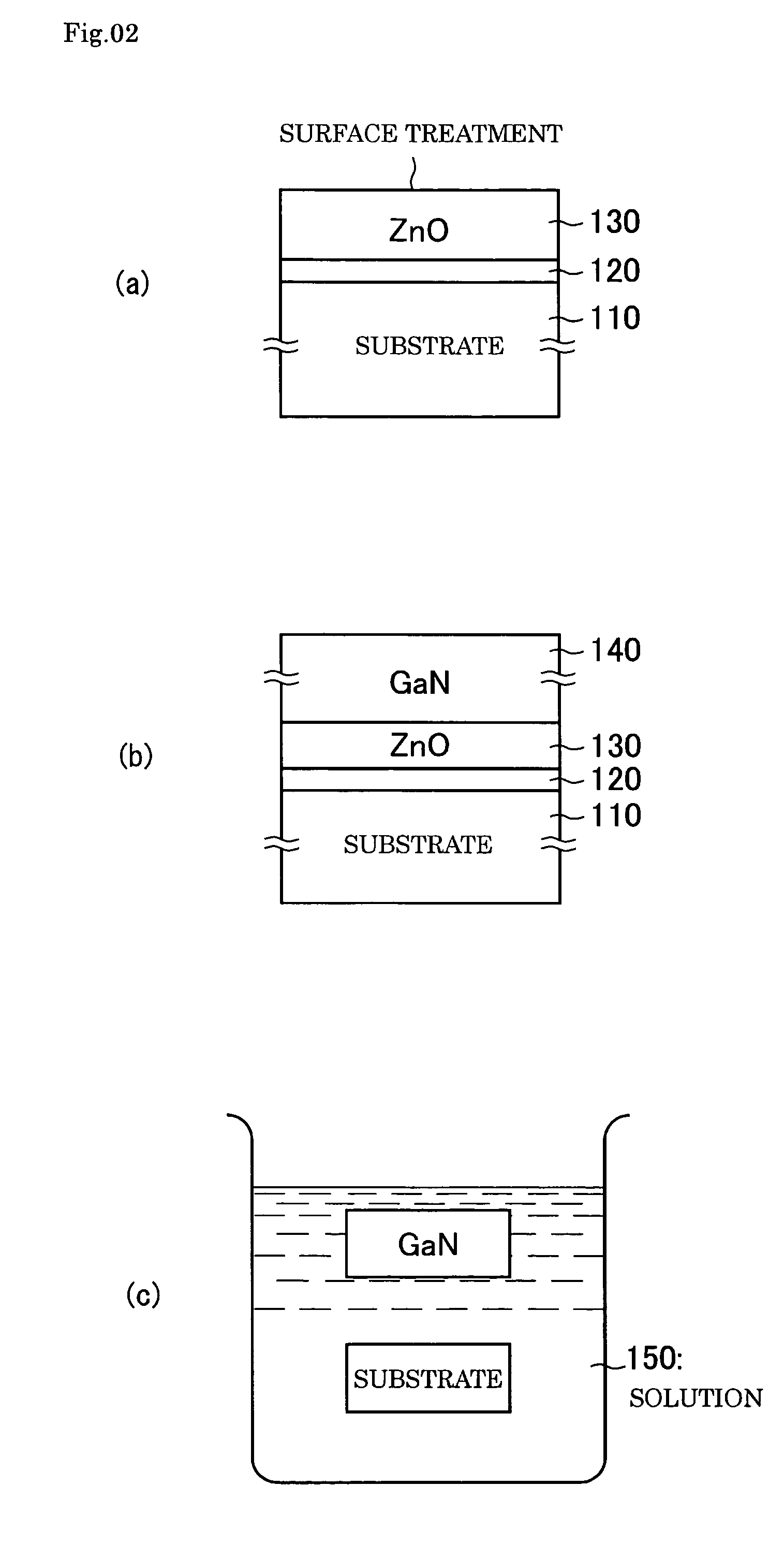
[0028]As an example, a procedure for producing a GaN substrate, using sapphire substrate as the high-quality substrate, is described in detail in reference to FIGS. 1 and 2.
[0029](1) A sapphire substrate (C-plane or A-plane) 110 is purified. A well-known purification method can be adapted therefor (refer to FIG. 1(a)).
[0030](2) A MgO single crystal thin film (buffer layer) 120 at 2 nm or less thick is deposited thereon. This growth was carried out in...
PUM
| Property | Measurement | Unit |
|---|---|---|
| thick | aaaaa | aaaaa |
| temperature | aaaaa | aaaaa |
| temperature | aaaaa | aaaaa |
Abstract
Description
Claims
Application Information