Programmable electronic fuse

a technology of electronic fuse and programmable components, applied in the direction of semiconductor devices, semiconductor/solid-state device details, electrical equipment, etc., can solve the problems of requiring additional process steps including mask levels and lithographic processes

Active Publication Date: 2009-02-03
INT BUSINESS MASCH CORP
View PDF40 Cites 20 Cited by
  • Summary
  • Abstract
  • Description
  • Claims
  • Application Information

AI Technical Summary

Benefits of technology

[0005]The present invention overcomes this and other drawbacks by employing a device or fuse structure of composite layers of materials that migrate by a specific type of physical diffusion process under an applied current. This differs from the melting or vaporizing type common with many known fuses during a programming event. The material (e.g., CoSi2 or NiSi2) that visually migrates (mostly by electromigration) causes the change in the resistance of the fuse, while not causing collateral damage during its migration or material reformation, and has a programmed state where ±ΔRp is preferably small and close to zero (i.e the programmed fuse resistances are tightly distributed). Thus, the present invention allows for individual fuses to discriminate among themselves on the basis of programming and to eliminate unwanted reference fuse elements, as well as the circuitry used to bias and compare against the reference fuse elements. A “reliable” eFuse technology in this application means a fuse structure and / or programming methodology that result in a large population of eFuses to achieve a programmed resistance objective (greater than some resistance value or a nominal value and a sigma etc.) without melting or other process that can cause collateral damage.
[0006]FIGS. 1A and 1B show a known generic fuse with a narrow and uniform middle portion, referred to as a fuse link or a fuse element, and wider fuse end parts which are contact regions. The fuse end parts are shown as symmetrical, but alternatively can be asymmetrical. The fuse has an underlying polysilicon layer and an overlying silicide layer. FIG. 2a shows a top view and FIG. 2b shows a cross sectional view of a fuse or programmable device according to one preferred embodiment of the present invention. According to a preferred embodiment of the present invention, a programmable device includes a semiconductor substrate (10); an insulator (13) on the substrate; an elongated semiconductor material (12) on the insulator, the elongated semiconductor material having first and second ends, a link region (11) and an upper surface S; the first end (12a) being substantially wider than the second end (12b), and a metallic material (40) on / at the upper surface, said metallic material being physically migratable along the upper surface responsive to an electrical current I passing through the elongated semiconductor material and the metallic material. Preferably, a nitride or other suitable barrier material is disposed on the surfaces of the fuse. The semiconductor material 12 is doped with p or n type impurities which have a concentration of at least 1017 / cc. Dopant concentrations equal to or greater than 1017 / cc provide the reliability and other benefits of the present invention.
[0008]A method of programming an eFuse according to the present invention includes flowing an electrical current I through the fuse having a metallic material such as a semiconductor alloy (40) disposed on a doped semiconductor line (12), for a time period such that a portion of the semiconductor alloy migrates from a first end (12a) of the device to a location proximate to a second end (12b) of the device. Further, the inventors believe that the dopants in portions of the doped semiconductor line 12 are removed during the programming cycle enabling a high final resistance.
[0010]Accordingly, it is an object of the present invention to provide a method of fabricating a reliable programmable eFuse, which method is readily compatible with various standard MOS manufacturing processes, including those used for DRAM and Logic devices.
[0011]An additional object of the present invention is to provide a method of programming an eFuse which reduces collateral damages to neighboring structures.
[0012]Another object of the present invention is to provide a reliable eFuse design that can be programmed using low voltages of 5 volts and less.

Problems solved by technology

The disadvantage of this eFuse ('601) is that in order to create such a structure, additional process steps including mask levels and lithographic processes are required.

Method used


Image

  • Programmable electronic fuse
  • Programmable electronic fuse
  • Programmable electronic fuse

Examples


Embodiment Construction

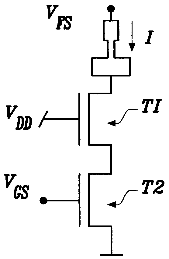
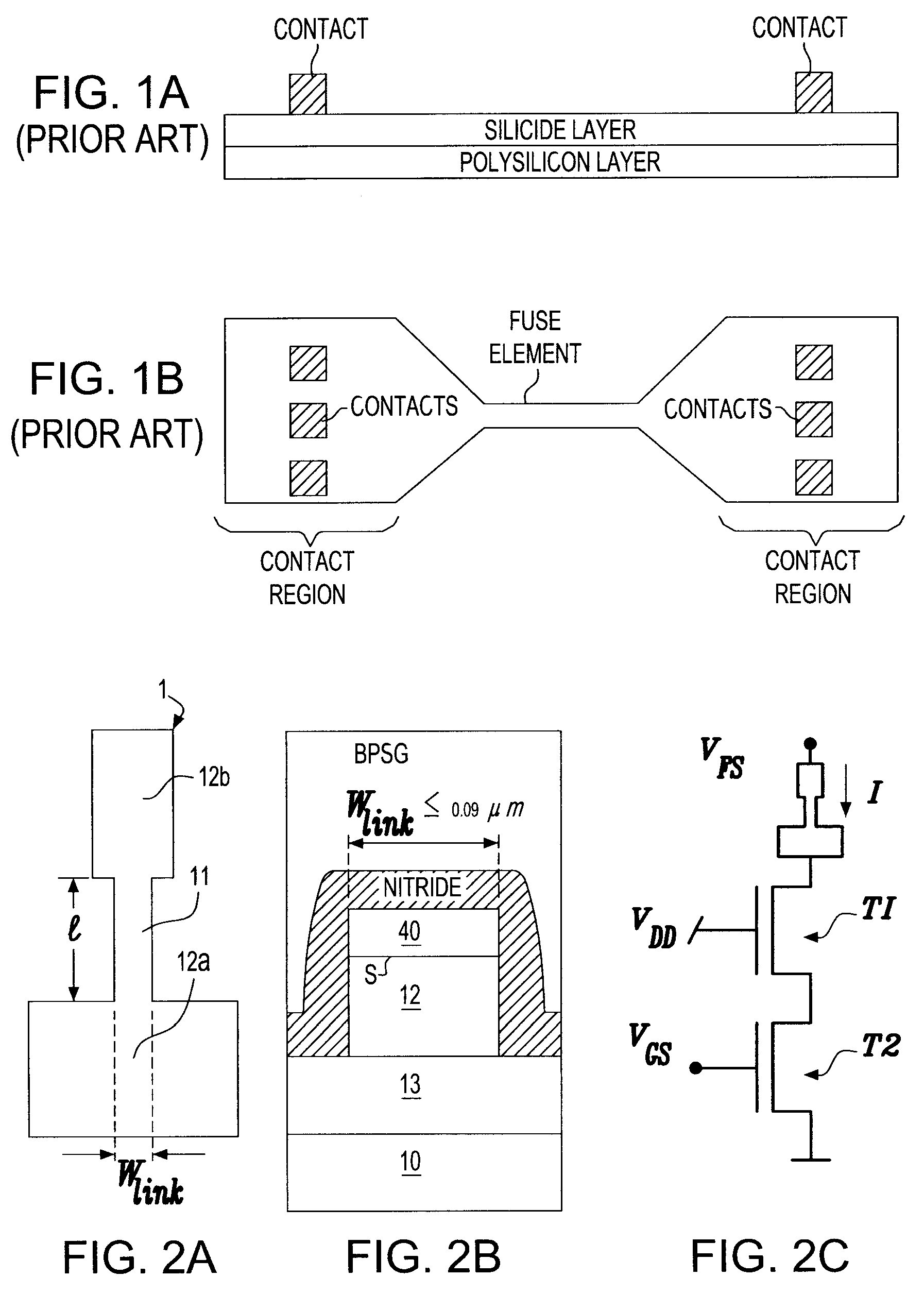
[0032]FIG. 2a is a top view of a fuse according to the present invention, wherein the fuse ends 12a, 12b are asymmetrical. The fuse link portion has an approximately (±10%) uniform width W. Following the terminology used in semiconductor technologies, a square is used to denote a film of equal width and length; the fuse length can be viewed as made of several squares of the fuse material. The nominal minimum width W of the fuse link corresponds to the technology node scale used. For example, if one uses 90 nm technology then the nominal width W of the fuse link 11 is therefore 90 nm. FIG. 2b shows a cross sectional view of the fuse and its placement (for example) in a CMOS semiconductor chip. The fuse link is situated over an insulator, in this case over an isolation oxide (13). The fuse itself includes a bottom layer 12 of polysilicon and a top layer 40 of metallic material. Preferably, the cathode (12a) and the anode (12b) have dissimilar shapes and have larger cross sections than...


PUM


Abstract

A programmable device (eFuse), includes: a substrate (10); an insulator (13) on the substrate; an elongated semiconductor material (12) on the insulator, the elongated semiconductor material having a first end (12a), a second end (12b), a fuse link (11) between the ends, and an upper surface S. The semiconductor material includes a dopant having a concentration of at least 10*17 / cc. The first end (12a) is wider than the second end (12b), and a metallic material is disposed on the upper surface. The metallic material is physically migratable along the upper surface responsive to an electrical current I flowable through the semiconductor material and through the metallic material.

Description

TECHNICAL FIELD[0001]The present invention relates to programmable semiconductor devices and, more particularly, to such devices usable as semiconductor electronic fuses (eFuses).BACKGROUND ART[0002]Semiconductor eFuses in general are known. The word fuse or eFuse will be used interchangeably in this specification. Specifically, eFuse in this application refers to fuses that increase the resistance of a circuit path when subjected to a programming current.[0003]However, known eFuses have not proven to be entirely satisfactory. Programming in, for example, silicon-based semiconductor devices (e.g., fuses) can result in post collateral damage of neighboring structures. This result typically forces a fuse pitch, or fuse cavity, set of rules that do not scale well with the technology feature rules from one generation to the next. Thus, fuse density and effectiveness of fuse repair, replacement, or customization are limited. Typically, such damage is caused by particulates from fuse blow...

Claims


Application Information

Patent Timeline
Patent Type & Authority Patents(United States)
IPC IPC(8): H01L23/525
CPCH01L23/5256H01L2924/0002H01L2924/00
Inventor KOTHANDARAMAN, CHANDRASEKHARANIYER, SUBRAMANIAN
Owner INT BUSINESS MASCH CORP
Why Eureka
Try Eureka