Memory module testing apparatus and method of testing memory modules

a memory module and testing apparatus technology, applied in the direction of instruments, biological water/sewage treatment, inclination control of settling devices, etc., can solve the problem that the conventional memory module testing apparatus cannot test 16 2-rank sodimm products

Active Publication Date: 2009-02-03
SAMSUNG ELECTRONICS CO LTD
View PDF10 Cites 7 Cited by
  • Summary
  • Abstract
  • Description
  • Claims
  • Application Information

AI Technical Summary

Problems solved by technology

Because the occurrence of a failure in a memory device may cause a fatal error in a system operation in the system in which the memory device is used, manufactured memory devices are tested in a system (e.g., a motherboard) that simulates their actual working environment before being released into the market.
However, when a conventional memory module testing apparatus tests a SODIMM, a motherboard using a standard DIMM only supports ×8 1-rank, ×8 2-rank, and ×16 1-rank SODIMM products without supporting ×16 2-rank SODIMM products.
As a result, the conventional memory module testing apparatus cannot test ×16 2-rank SODIMM products.

Method used


Image

  • Memory module testing apparatus and method of testing memory modules
  • Memory module testing apparatus and method of testing memory modules
  • Memory module testing apparatus and method of testing memory modules

Examples


Embodiment Construction

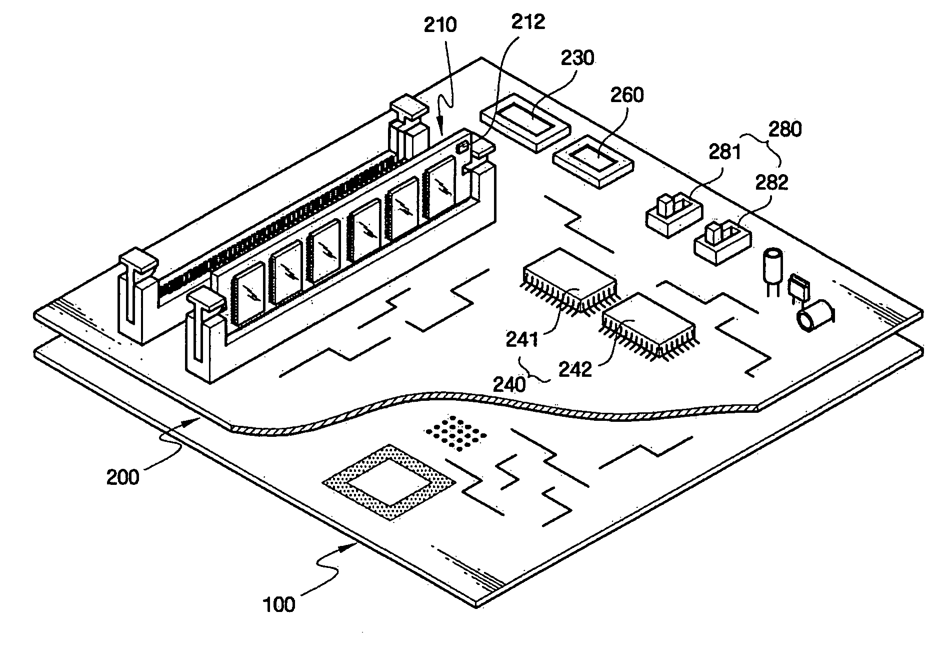
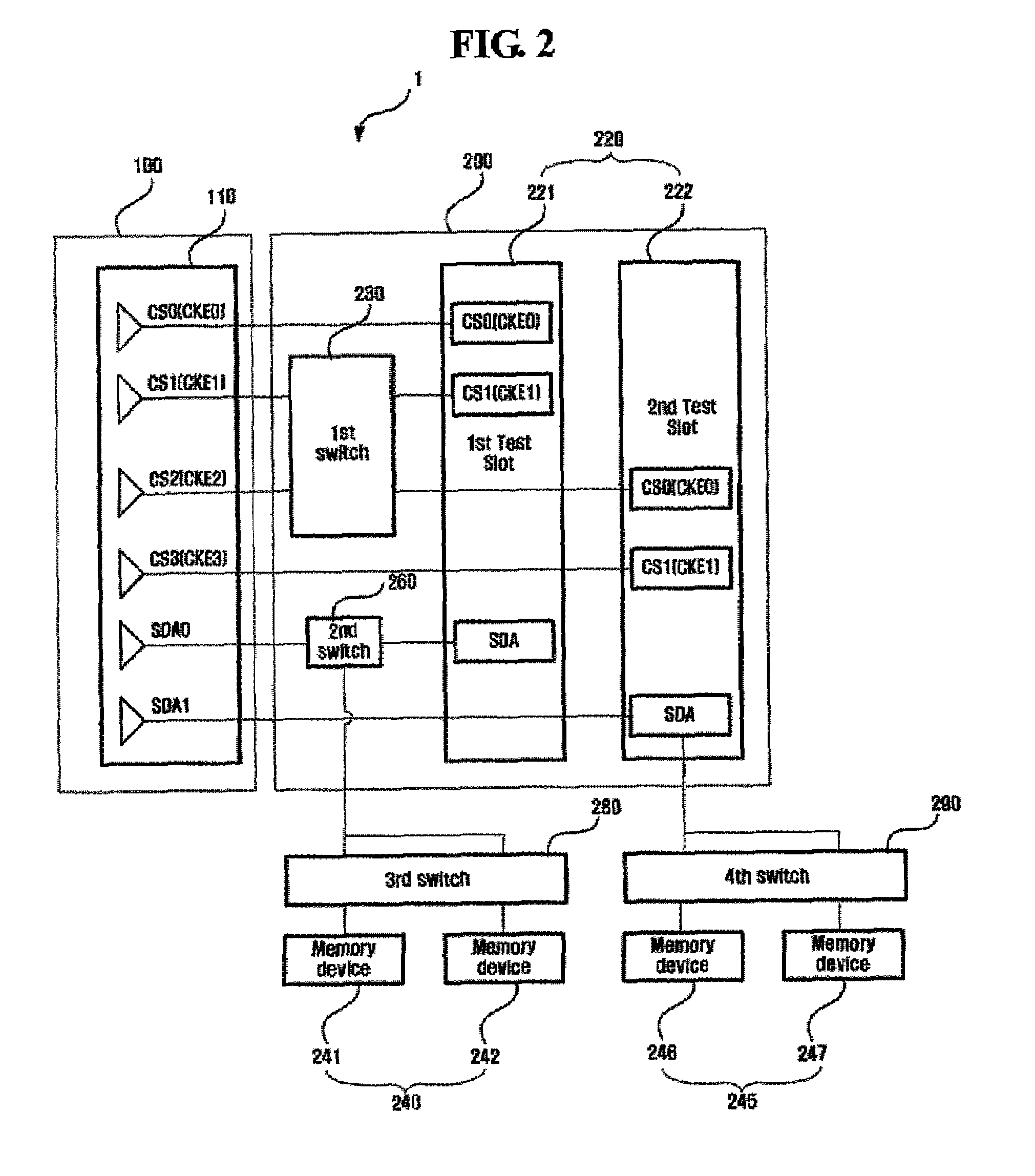
[0020]FIG. 1 is a perspective view of a memory module testing apparatus in accordance with an exemplary embodiment of the present invention, and FIG. 2 is a block diagram of a memory module testing apparatus in accordance with an exemplary embodiment of the present invention.

[0021]The structure of interface board 200 shown in FIG. 1 is only an exemplary structure for interface board 200. The structure of interface board 200 can take various forms in accordance with the environment in which a target memory module 210 is used, wherein target memory module 210 is the memory module that will be tested using the memory module testing apparatus of FIG. 1. For simplicity, a detailed configuration of interface board 200 is omitted in FIG. 1.

[0022]Referring to FIGS. 1 and 2, a memory module testing apparatus 1 comprises a motherboard 100 and interface board 200.

[0023]Motherboard 100 may take any form that can be used in a device in which target memory module 210 can be mounted, such as a des...


PUM


Abstract

A memory module testing apparatus and method include a test slot adapted to receive a target memory module, wherein the target memory module includes a first memory unit to store information related to the target memory module. The memory module testing apparatus further includes a second memory unit adapted to store information related to a memory module, and a first switching unit adapted to selectively provide a driving signal to at least one of the first memory unit and the second memory unit.

Description

BACKGROUND OF THE INVENTION[0001]1. Field of the Invention[0002]Embodiments of the invention relate to a memory module testing apparatus. In particular, embodiments of the invention relate to a memory module testing apparatus capable of testing various types of memory modules.[0003]This application claims priority to Korean Patent Application No. 10-2005-0029093, filed on Apr. 7, 2005, the subject matter of which is hereby incorporated by reference in its entirety.[0004]2. Description of the Related Art[0005]A memory device is a storage device used to temporarily or permanently store data used in a digital logic system. Because the occurrence of a failure in a memory device may cause a fatal error in a system operation in the system in which the memory device is used, manufactured memory devices are tested in a system (e.g., a motherboard) that simulates their actual working environment before being released into the market.[0006]In general, a conventional motherboard used to test m...

Claims


Application Information

Patent Timeline
Patent Type & Authority Patents(United States)
IPC IPC(8): G11C29/00
CPCG11C5/04G11C29/56C02F3/34C02F3/327C02F1/52B01D21/0015B01D21/0003C02F1/28E01F5/00C02F2103/001E03F2201/10
Inventor LEE, JUNG-KUKSEO, SEUNG-JINHAN, YOU-KEUNSHIN, SEUNG-MANAHN, YOUNG-MAN
Owner SAMSUNG ELECTRONICS CO LTD
Why Eureka
Try Eureka