Memory module with offset data lines and bit line swizzle configuration

a memory module and offset data technology, applied in the field of memory systems, can solve problems such as the multiplication of memory devices to respond to the problem of memory device offs

Inactive Publication Date: 2005-01-04
RAMBUS INC
View PDF18 Cites 191 Cited by
  • Summary
  • Abstract
  • Description
  • Claims
  • Application Information

AI Technical Summary

Problems solved by technology

However, the same command, set of commands, instruction, or part of an instruction causes a p

Method used


Image

  • Memory module with offset data lines and bit line swizzle configuration
  • Memory module with offset data lines and bit line swizzle configuration
  • Memory module with offset data lines and bit line swizzle configuration

Examples


Embodiment Construction

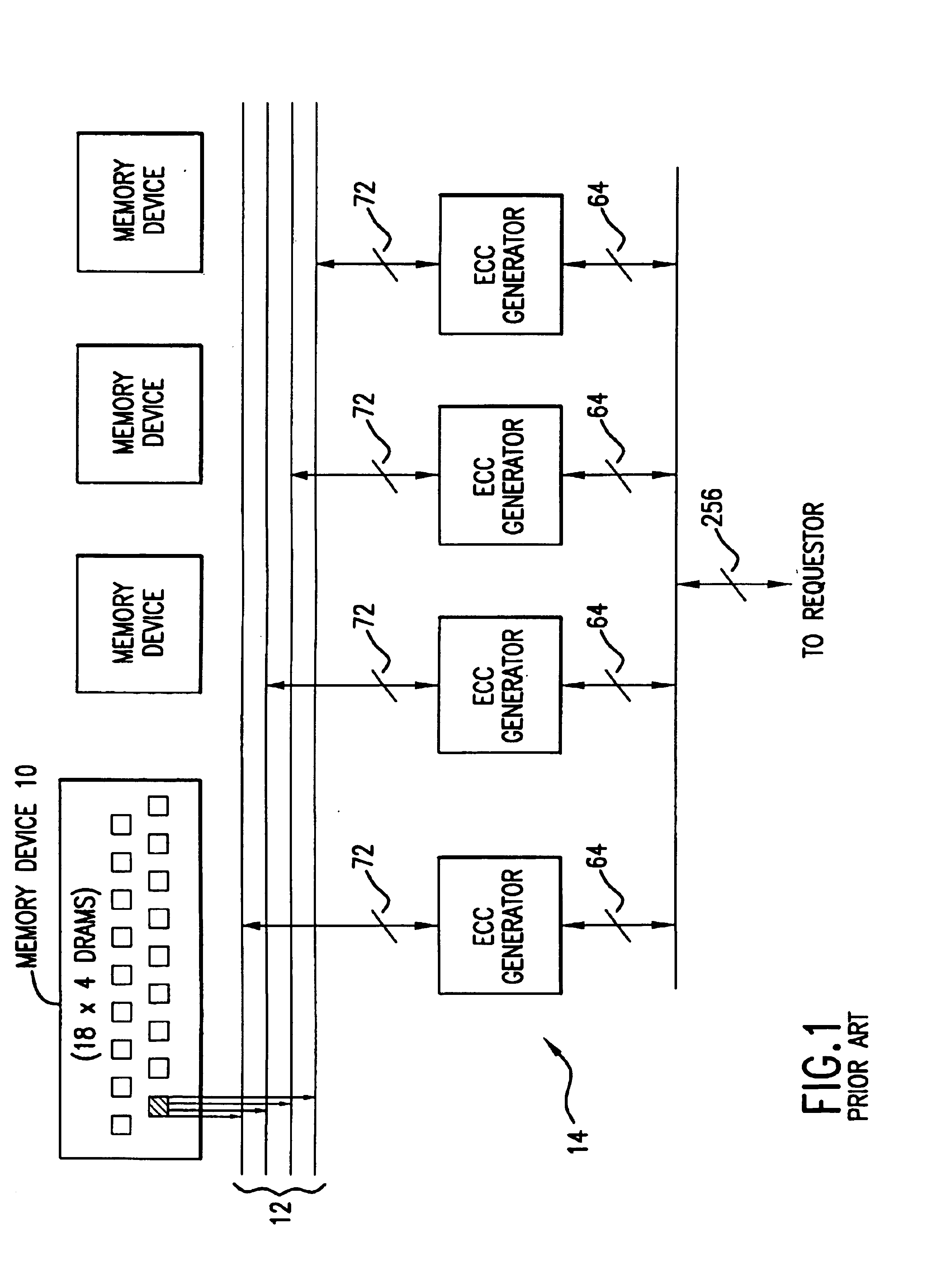
The assignee of the present invention has pioneered the development of next generation memory systems having a relatively narrow, high speed bus(es) and associated memory devices, along with the interface technology required to provide high data throughput. See, U.S. Pat. Nos. 5,319,755; 5,243,703; and 5,254,883, the disclosures of which are incorporated herein by reference.

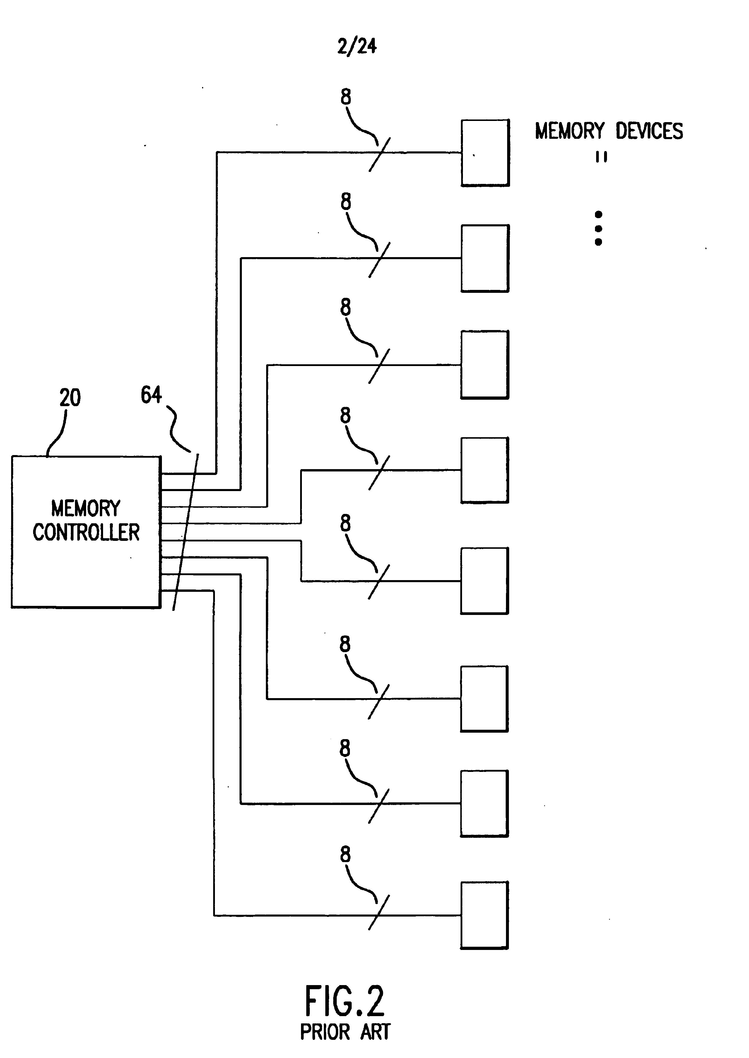
Very general differences between conventional memory systems and the assignee's memory systems can be seen by comparing FIGS. 2 and 3. In FIG. 2, eight 8-bit memory devices 11 are connected to a memory controller 20 by a 64-bit bus. Assuming 8-bit bytes and a system clock running at 100 MHz, the total data throughput for the conventional system is 800 MB / sec.

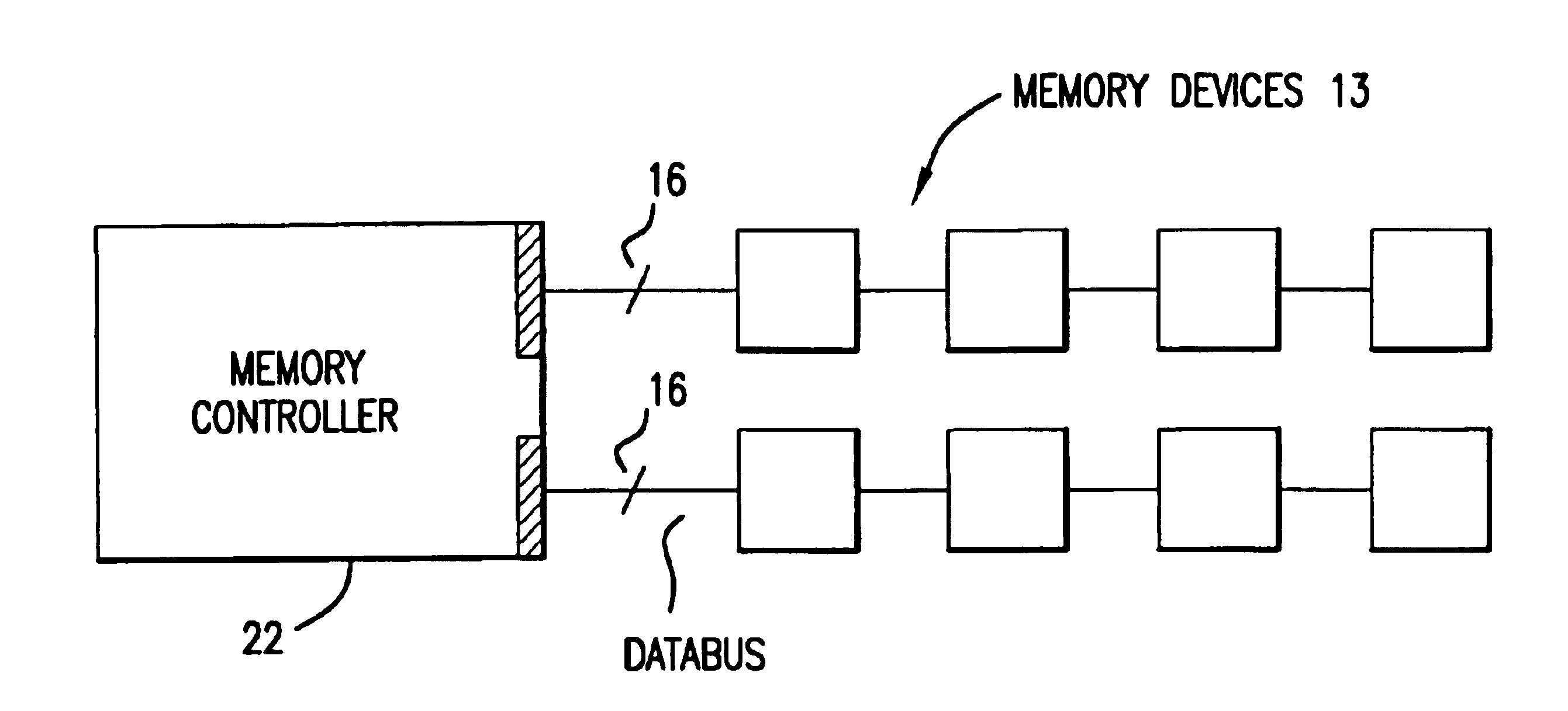
In FIG. 3, eight 8-bit memory devices according to the assignees design 13 are connected to a memory controller 22 by two 16 bit data buses. Since each of the assignee's memory devices is capable within the memory system architecture of communicating data on ...


PUM


Abstract

A memory module includes an array of N memory devices, each memory device having M data pins, where N is greater than M, and M and N are positive integers; and N bit lines traversing the array of N memory devices, such that each one of the N bit lines is connected to M of the N memory devices.

Description

FIELD OF THE INVENTIONA memory system characterized by high speed data throughput on a bus between a memory controller and an associated plurality of memory devices is disclosed, wherein the memory system is capable of selectively operating in non-chip-kill and chip-kill modes. A method of selectively operating the memory system is either non-chip-kill or chip-kill modes is also disclosed.BACKGROUND OF THE INVENTIONDuring the last several decades, memory technology has progressed dramatically. The density of commercial memory devices, taking Dynamic Random Access Memory (DRAM) as a convenient example, has increased from 1 Kbit to 64 Mbits per chip, a factor of 64,000. Unfortunately, memory device performance has not kept pace with increasing memory device densities. In fact, memory device access times during the same time period has only improved by a factor of 5. By comparison, during the past twenty years, microprocessor performance has increased by several orders of magnitude. Th...

Claims


Application Information

Patent Timeline
IPC IPC(8): G06F11/10G11C7/10G11C29/00
CPCG06F11/1028G11C7/1072G06F11/1044
Inventor GARRETT, JR., BILLY WAYNEWARE, FREDERICK ABBOTTHAMPEL, CRAIG E.BARTH, RICHARD M.STARK, DONABHYANKAR, ABHIJIT MUKUNDCHEN, CATHERINE YUHJUNGSHEFFLER, THOMAS J.TSERN, ELY K.WOO, STEVEN CAMERON
Owner RAMBUS INC
Why Eureka
Try Eureka