
Electron beam detection device and electron tube

a detection device and electron tube technology, applied in the direction of optical radiation measurement, tubes with screens, instruments, etc., can solve the problems of unfavorable separation of semiconductor devices and signal processing circuits, unfavorable response speed, etc., and achieve the effect of preventing the response of signals

Inactive Publication Date: 2009-02-17
HAMAMATSU PHOTONICS KK
View PDF37 Cites 0 Cited by
  • Summary
  • Abstract
  • Description
  • Claims
  • Application Information

AI Technical Summary

Benefits of technology

[0012]An object of the present invention is therefore to provide an electron beam detection device that is capable of preventing response speed from being decreased and reducing noise to thereby detect electrons with good response and high sensitivity and an electron tube that uses the electron beam detection apparatus.Arrangement Solving the Problem
[0039]According to the electron tube having the above configuration, the electro-optic converter is disposed near the semiconductor device. Therefore, the response of signals is prevented from being impaired. Electrical signals can be converted into optical signals without being deteriorated and supplied to an external circuit.

Problems solved by technology

Therefore, separate installation of the semiconductor device and signal processing circuit is unfavorable, in terms of response speed and in terms of signal quality which may be deteriorated due to noise.

Method used


Image

  • Electron beam detection device and electron tube
  • Electron beam detection device and electron tube
  • Electron beam detection device and electron tube

Examples


Embodiment Construction

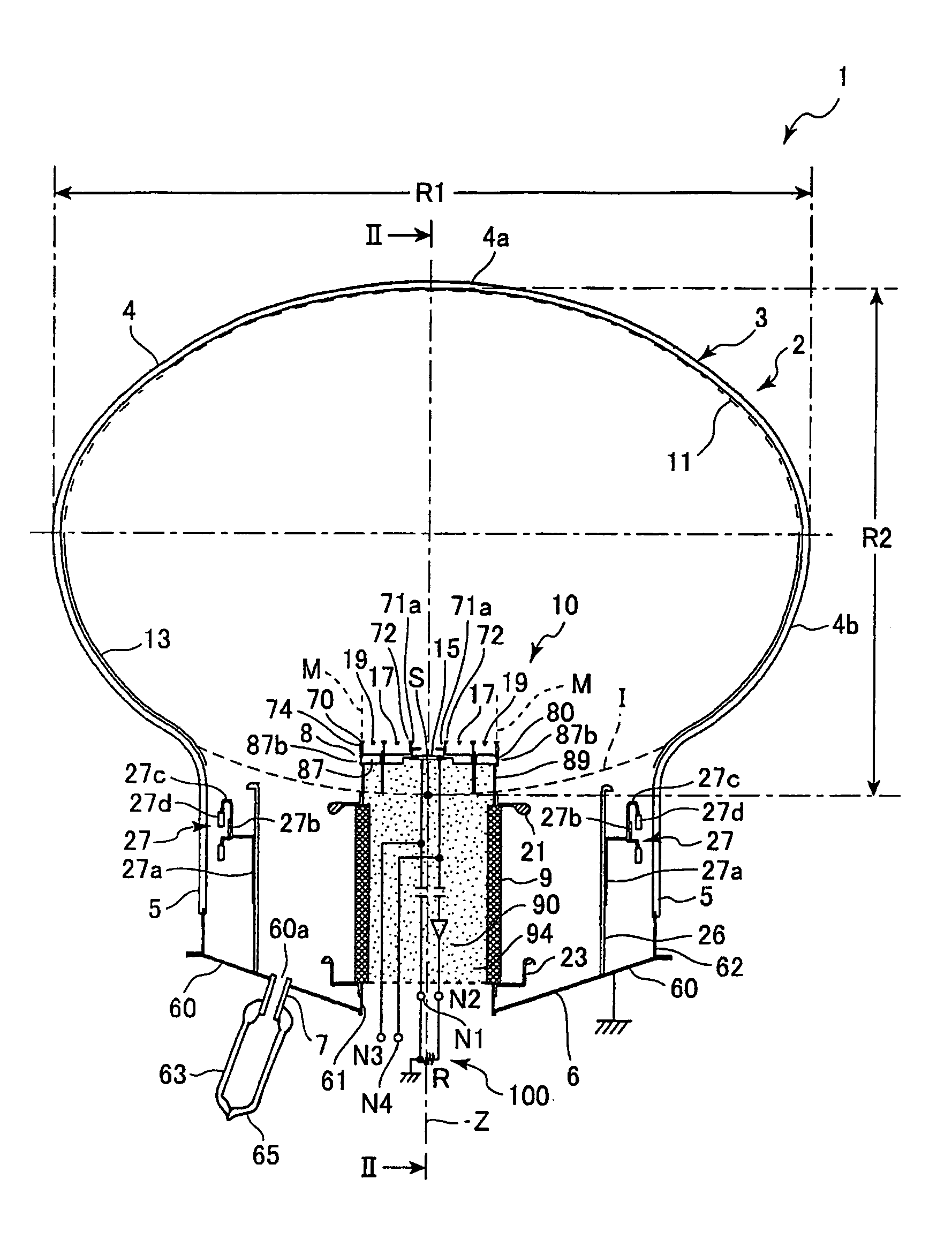
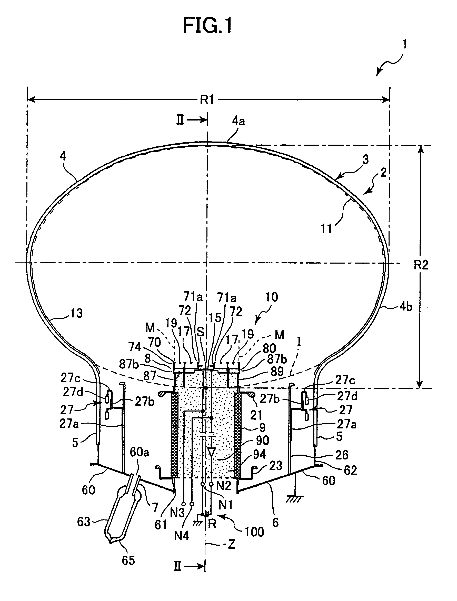
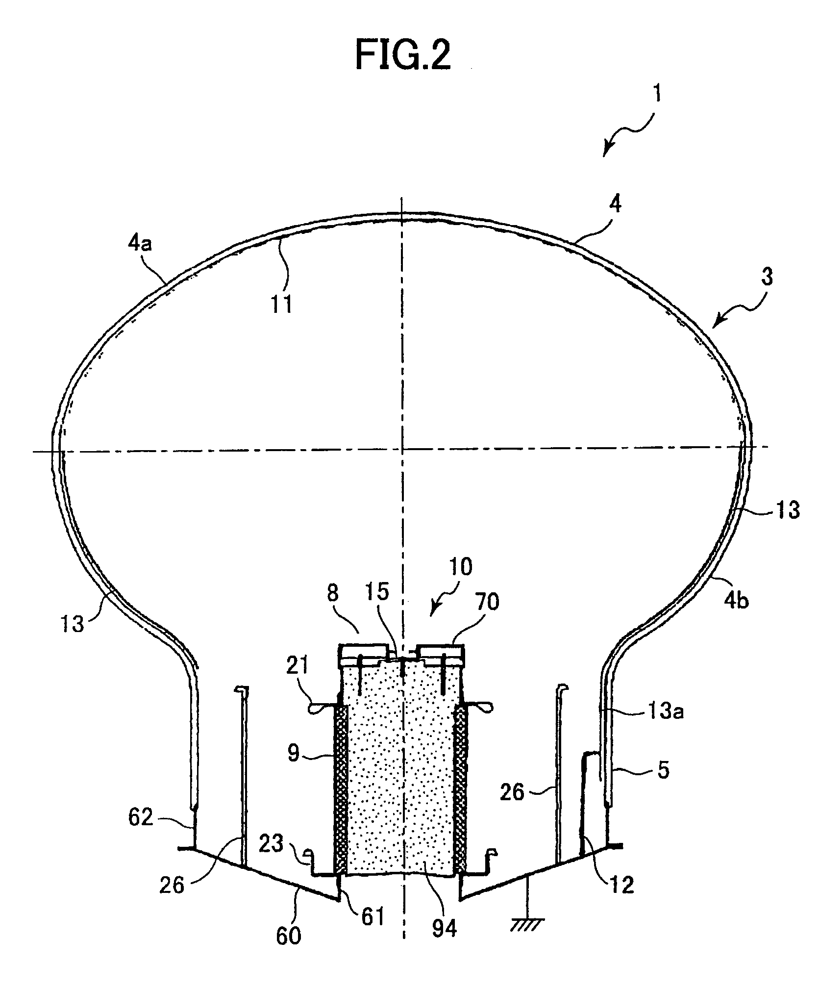
[0098]An electron tube according to an embodiment of the present invention will be described below with reference to FIGS. 1 to 17.

[0099]FIG. 1 is a vertical cross-sectional view schematically showing an electron tube 1 according to the embodiment of the present invention.

[0100]As shown in FIG. 1, the electron tube 1 includes an envelope 2 and an electron detection section 10. The envelope 2 has an axis Z. The electron detection section 10 protrudes inside the envelope 2 along the axis Z. The electron detection section 10 has substantially a cylindrical shape extending with its central axis being located on the axis Z.

[0101]The envelope 2 has a glass bulb 3 and an outer stem 6. The glass bulb 3 is formed from a transparent glass.

[0102]The glass bulb 3 has a glass bulb body 4 and a cylindrical glass bulb base 5. The glass bulb body 4 is integrally formed with the glass bulb base 5. The glass bulb body 4 has substantially a spherical shape having a central axis located on the axis Z. ...


PUM


Abstract

An insulating tube has one end and another end. An avalanche photodiode (APD) is provided outside the one end of the insulating tube. The another end of the insulating tube is air-tightly connected to an outer flange through a stem inner wall. Capacitors electrically connected to the APD are provided in the insulating tube. The capacitors remove direct current components from signals that the APD generates when detecting electrons. By providing the capacitors in the insulating tube, response of output signals can be prevented from being impaired.

Description

TECHNICAL FIELD[0001]The present invention relates to an electron beam detection device and an electron tube.BACKGROUND ART[0002]Various electron tubes have been proposed. The electron tube have a photocathode that emits photoelectrons in response to an incident light and an electron-bombarded semiconductor device, such as an avalanche photodiode (hereinafter, referred to as APD) that amplifies the photoelectrons so as to detect them.[0003]As an electron tube using the APD, there has been proposed an electron tube having an entrance window inside of which a photocathode is formed and a conductive stem on which the APD is disposed. The entrance window is provided at the opening of an insulating container, and the conductive stem is provided opposed to the photocathode of the insulating container. A signal output from the APD is input to an electrical circuit provided outside the insulating container through a lead pin and thereby the incident electrons are detected. The electrical ci...

Claims


Application Information

Patent Timeline
Patent Type & Authority Patents(United States)
IPC IPC(8): H01J40/14H01J31/50G01J1/02G01J1/42G01T1/24G01T1/28H01J1/35H01J37/244H01J43/12H01J43/16H01J43/30
CPCH01J40/14H01J43/30H01J2237/244
Inventor KYUSHIMA, HIROYUKISUYAMA, MOTOHIROKIMURA, SUENORINEGI, YASUHARUKAWAI, YOSHIHIKOFUKASAWA, ATSUHITO
Owner HAMAMATSU PHOTONICS KK
Learn More