Self-emitting element, display panel, display apparatus, and method of manufacturing self-emitting element

a technology of self-emitting elements and display panels, which is applied in the direction of discharge tubes luminescnet screens, identification means, instruments, etc., can solve the problems of reducing the efficiency of light, and affecting the output light of transparent electrode layers. , the effect of reducing contras

Active Publication Date: 2009-02-17
ELEMENT CAPITAL COMMERCIAL CO PTE LTD
View PDF34 Cites 17 Cited by
  • Summary
  • Abstract
  • Description
  • Claims
  • Application Information

AI Technical Summary

Benefits of technology

[0030]Even if an output layer having a high refractive index is prepared, if an intermediate layer having a refractive index smaller than that of the light-emitting element is disposed between the light-emitting element and the output layer, the light incident on the output layer is reduced by a component that undergoes total reflection at the interface of the intermediate layer. On the other hand, even if an intermediate layer having a refractive index greater than that of the output layer is disposed between the light-emitting element and the output layer, the light emitted from the light-emitting layer is incident on the output layer at less than the critical angle through the intermediate layer. Therefore, there is no loss of light in the intermediate layer. For this reason, it is necessary that the refractive index of the intermediate layer is greater than that of the light-emitting layer. If the light-emitting element is an organic EL that emits light when a voltage is applied, it is necessary to deposit a transparent layer, which is an electrode for applying voltage to the light-emitting element, on the display layer. This transparent electrode layer becomes an intermediate layer between the light-emitting element and the output layer. Therefore, by making the refractive index of this transparent electrode layer greater than that of the light-emitting element, the loss of the output light in the transparent electrode layer can be minimized.
[0031]On the other hand, when the difference between the refractive indices of the output layer and the transparent electrode layer is high, there is a reflection of light at an interface of the output layer and the transparent electrode layer due to difference in the refractive index and the efficiency of light is reduced. Moreover, when an external light is incident, due to reflection of the external light at the interface, the contrast is reduced. Therefore, it is desirable to improve the efficiency of light by providing an anti-reflective layer in the interface between the transparent electrode layer and the output layer and also minimize the reflection of the external light.
[0032]Light output from the output layer functions effectively when passing through air (refractive index of air is approximately one) and reaching eyes of a user. A transparent sealing layer may be provided in the direction of emission of the output layer across a space from the output layer. In this case, even if the space is filled with an inert gas having a refractive index of approximately one and the sealing layer is formed by a material having a refractive index of approximately 1.5, all the light input from the output layer to an inert gas layer can be input to the sealing layer. Further, since the refractive indices of the inert gas layer and an air layer on the user side are almost the same, all the light input to the sealing layer can be extracted in air.
[0033]In the present invention, in addition to adoption of the thin protective layer, the refractive index of the output layer is made same or greater than that of the light-emitting element. By doing so, the light extraction efficiency can be improved further.
[0034]Thus, the self-emitting element (display object) according to the present invention can improve further the efficiency of the light emitted from the light-emitting element, thereby enabling to output light having high brightness. Therefore, a display panel in which a plurality of self-emitting elements (display objects) are arranged two dimensionally in a matrix form can provide sharp images having high brightness. Moreover, a display apparatus that includes the display panel according to the present invention and the drive unit that displays images by driving the light-emitting element of the display panel makes it possible to display even brighter image at low electric power.

Problems solved by technology

However, in such structures in which angle of light emitted from the light-emitting layer is changed by the inclined surface portions and thereby total reflection in the interface is inhibited, the display panel is susceptible to become thick.
This may impose restriction on making of a very thin flat panel display.
This results in thickening of the transparent panel.
This results in deteriorating the light extraction efficiency.
Furthermore, the structure to change the angle of the light does not allow all the light emitted from the light-emitting element to be output from the display panel to the external medium.
Therefore, out of the light emitted from the light-emitting element, the light having an angle of incidence on the glass substrate not less than the critical angle is reflected at the boundary of the glass substrate and this light cannot be extracted.
Therefore, the light extraction efficiency cannot be improved.

Method used


Image

  • Self-emitting element, display panel, display apparatus, and method of manufacturing self-emitting element
  • Self-emitting element, display panel, display apparatus, and method of manufacturing self-emitting element
  • Self-emitting element, display panel, display apparatus, and method of manufacturing self-emitting element

Examples


Embodiment Construction

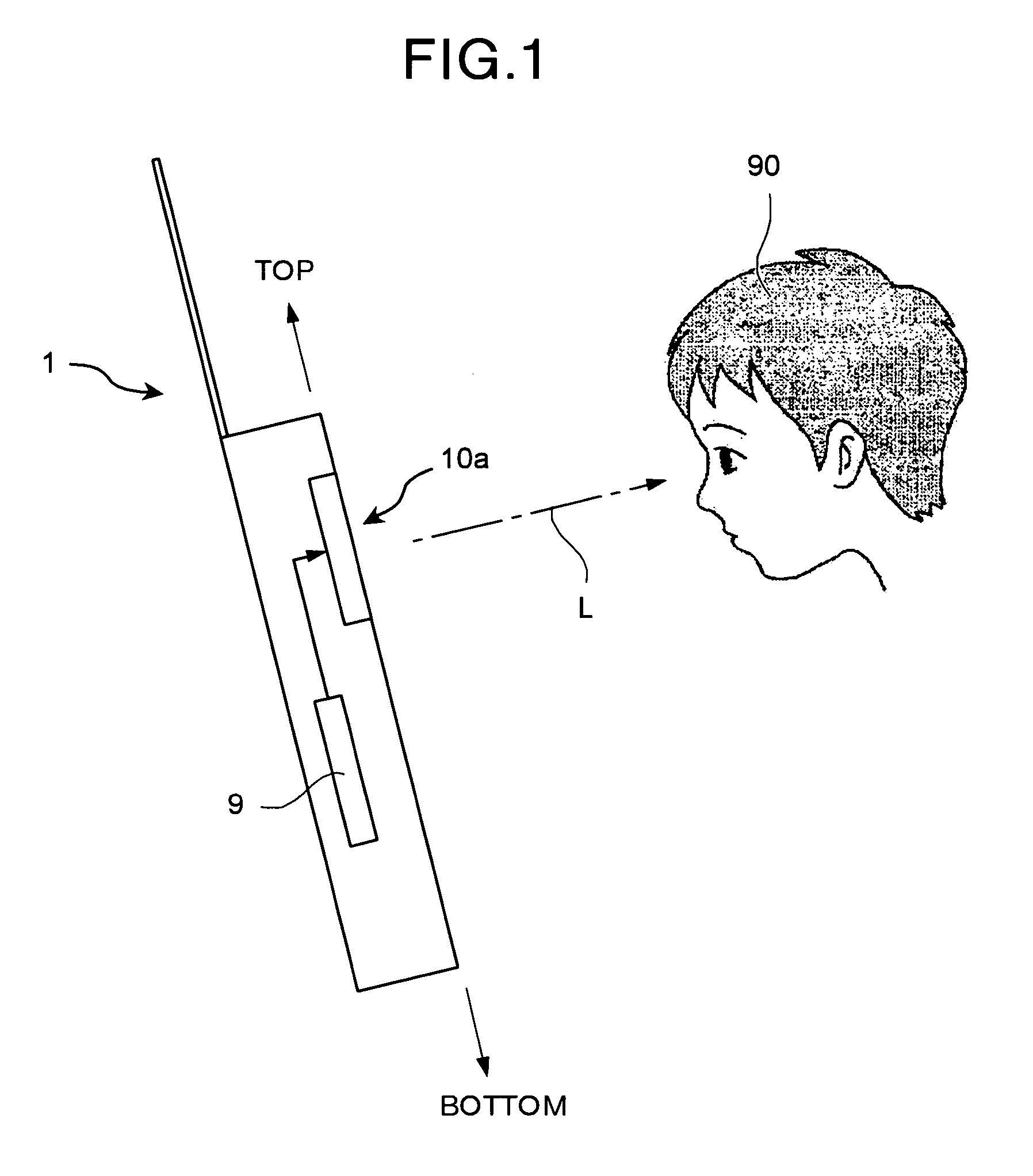
[0057]The present invention is explained in detail below with reference to the accompanying drawings. FIG. 1 is a diagram of a portable telephone as a display apparatus in which a display panel according to the present invention is installed. A portable telephone 1 in this embodiment includes a display panel 10a on which data is displayed and a drive unit 9. The display panel 10a includes organic EL elements which is self-emitting elements. The drive unit 9 that includes a micro computer causes the organic EL element to emit light L and a user 90 views data that includes characters and images.

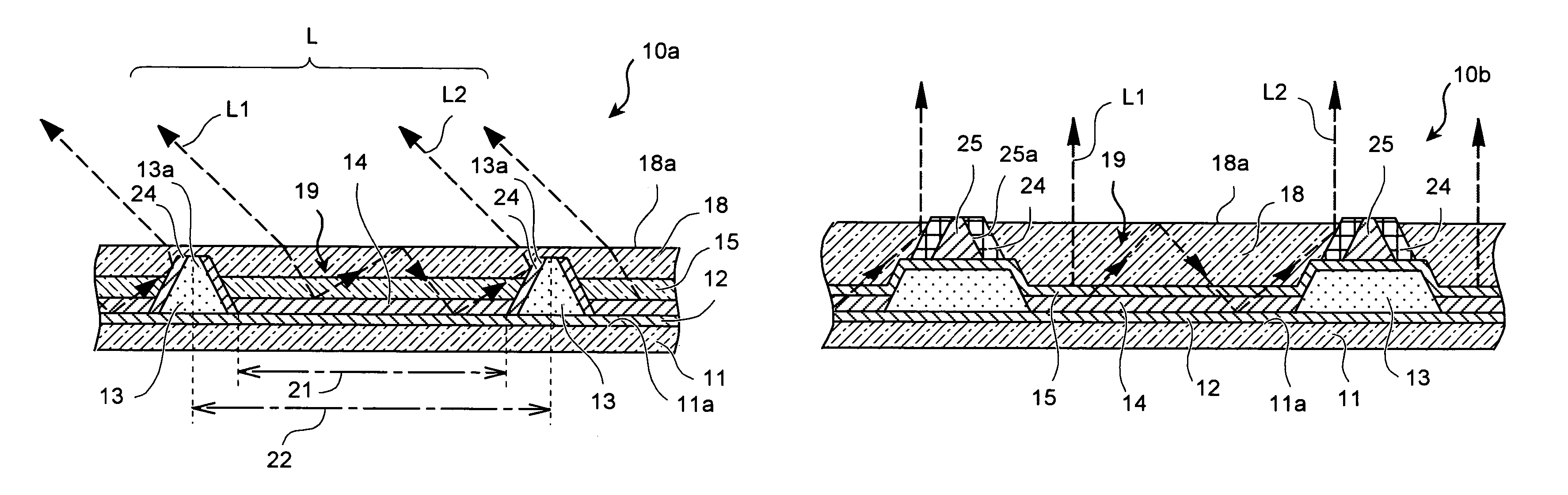
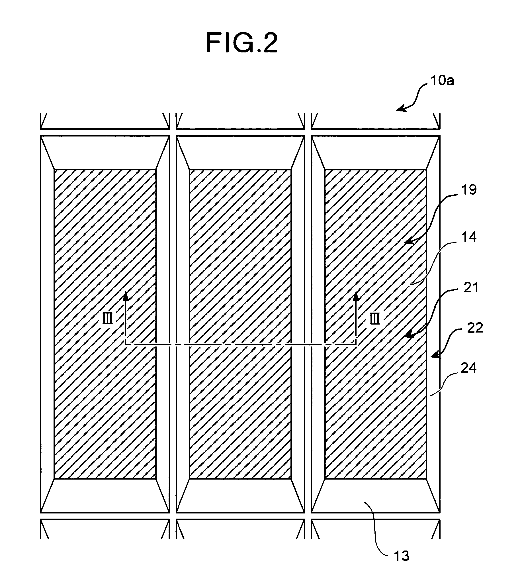
[0058]FIG. 2 is a top view of the display panel in an enlarged form. FIG. 3 is a cross sectional view of a striped area III. The display panel 10a in this embodiment is formed by disposing a plurality of pixels from the organic EL elements in a matrix form and can be driven by an active matrix or by a passive matrix. The display panel 10a includes a plurality of display objects 19 or a self-emi...


PUM


Abstract

A display panel includes a light-emitting layer, a protective layer, a reflective layer, and a reflective surface. The protective layer is deposited on an emitting side of the light-emitting layer and forms an interface with an external medium. The protective layer has a thickness that allows the light emitted from the light-emitting layer to undergo total reflection at least once at the interface in an area of the light-emitting layer. The reflective layer is deposited on an opposite side of the protective layer with respect to the light-emitting layer. The reflective surface is at a periphery of the light-emitting layer and changes the direction of the light propagating inside the protective layer emitted from the light-emitting layer.

Description

CROSS-REFERENCE TO RELATED APPLICATIONS[0001]This application is based upon and claims the benefit of priority from the prior Japanese Patent Applications No. 2002-365522 filed on Dec. 17, 2002 and No. 2003-049396 filed on Feb. 26, 2003; the entire contents of which are incorporated herein by reference.BACKGROUND OF THE INVENTION[0002]1) Field of the Invention[0003]The present invention relates to a self-emitting element like an organic electro-luminescent element (hereinafter, “organic EL element”), a display panel, a display apparatus, and a method of manufacturing the self-emitting element.[0004]2) Description of the Related Art[0005]In recent years, self-emitting flat panel displays (hereinafter, “FPD”) in which display panels including light-emitting elements (e.g., organic EL elements) or plasma display panels (hereinafter, “PDP”) are used have been developed. Such display panels include a light-emitting layer disposed between an anode electrode and a cathode electrode. The li...

Claims


Application Information

Patent Timeline
Patent Type & Authority Patents(United States)
IPC IPC(8): H01J1/62H01J63/04H05B33/22G09F9/30H01L27/32H01L51/52
CPCH01L27/3246H01L27/3283H01L51/5275H01L51/5271H01L51/5237H01L2251/5315H01L51/5281H10K59/173H10K59/122H10K50/858H10K50/856H10K50/86H10K50/844H10K2102/3026H05B33/22
Inventor YAMAUCHI, TAISUKE
Owner ELEMENT CAPITAL COMMERCIAL CO PTE LTD
Why Eureka
Try Eureka