Electrical Inspection of Electronic Devices Using Electron-Beam Induced Plasma Probes

Inactive Publication Date: 2014-05-15
ORBOTECH LTD +1
View PDF4 Cites 5 Cited by
  • Summary
  • Abstract
  • Description
  • Claims
  • Application Information

AI Technical Summary

Benefits of technology

The patent is for a device that measures signals without touching the structure being tested. The device has a feature to reduce the amount of light that affects the measurements. This helps to improve the accuracy of the data values.

Problems solved by technology

They may roughly be divided into two categories, one category being based on high intensity laser-induced ionization, which presents possible risks of laser-induced damage to the device under tests given the high ionization thresholds, and another category being based on high voltage corona discharges, in which ionized species have a wide range of scattering angles and also presents damage risks, especially related to arcing.

Method used


Image

  • Electrical Inspection of Electronic Devices Using Electron-Beam Induced Plasma Probes
  • Electrical Inspection of Electronic Devices Using Electron-Beam Induced Plasma Probes
  • Electrical Inspection of Electronic Devices Using Electron-Beam Induced Plasma Probes

Examples


first embodiment

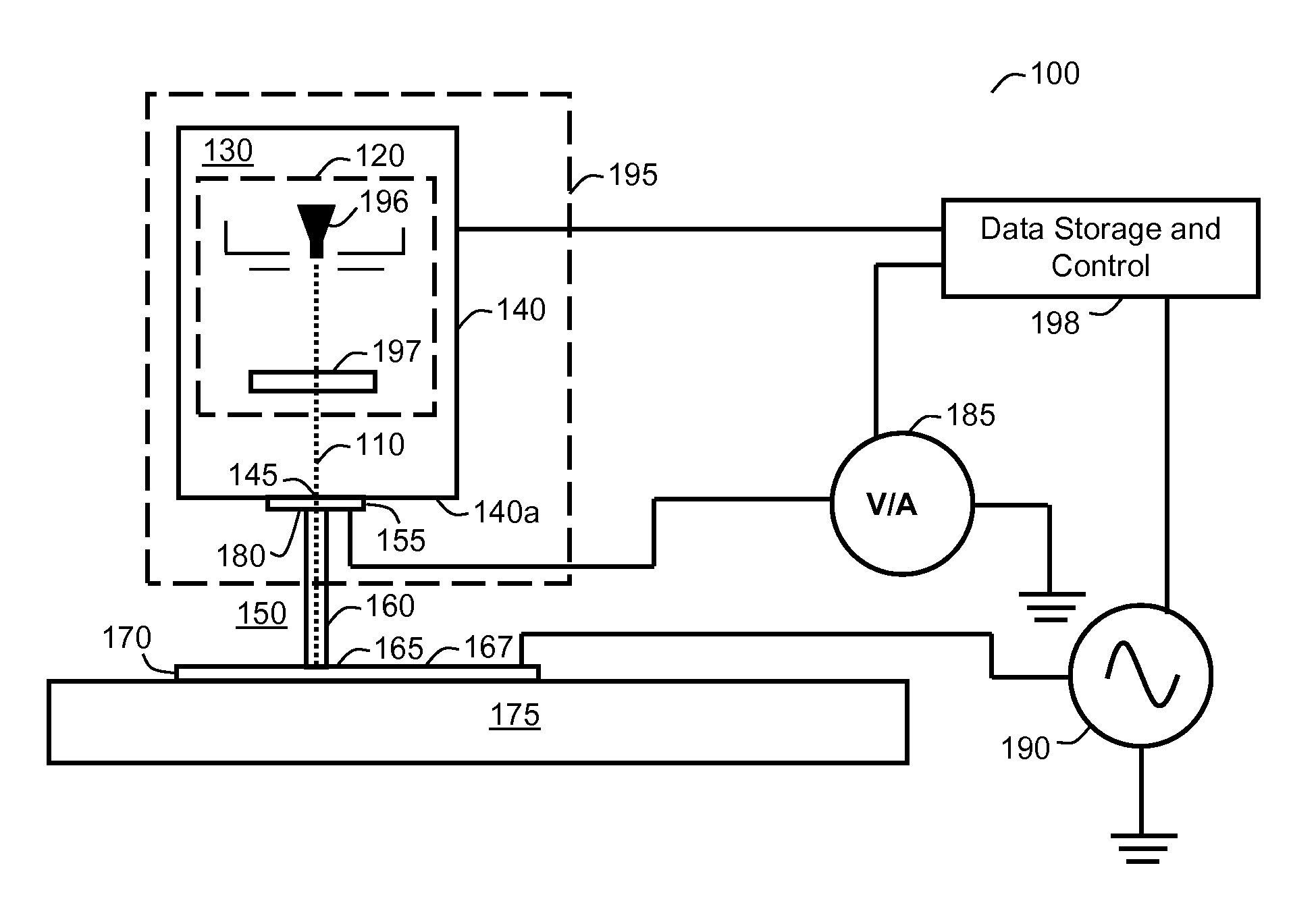
[0038]FIG. 1 is a schematic and cross sectional view of a non-mechanical contact signal measurement apparatus 100, in accordance with the present invention. An electron beam 110 is generated by an electron beam generator 120 in a vacuum 130 using conventional methods. Electron beam 110 egresses a vacuum enclosure 140 (hereinafter alternatively referred to as vacuum chamber) through an orifice 145 located in a portion of the vacuum enclosure 140a. A portion of the electron beam is passed to an ambient gas 150 (hereinafter alternatively referred to as ambient or gas) outside the vacuum enclosure through a membrane and frame assembly 155 that preserves the vacuum inside the vacuum enclosure containing the electron beam generator but is semi-transparent to the electron beam. Alternatively, membrane and frame assembly 155 may be optional when the orifice or multiplicity of orifices is small enough to preserve the vacuum inside the vacuum enclosure.

[0039]Upon entering the ambient gas, the...

second embodiment

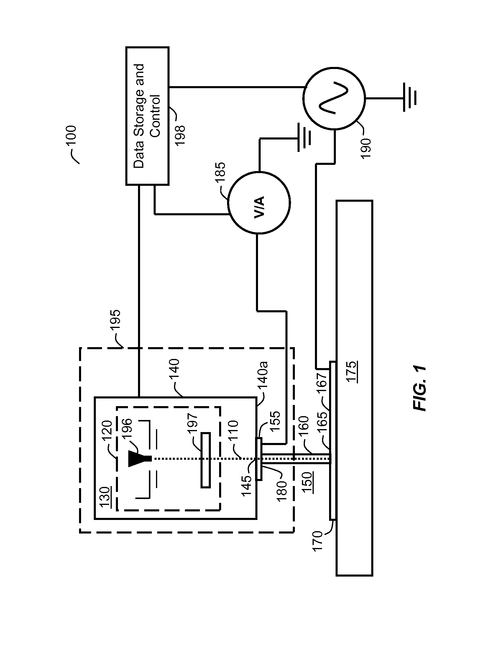
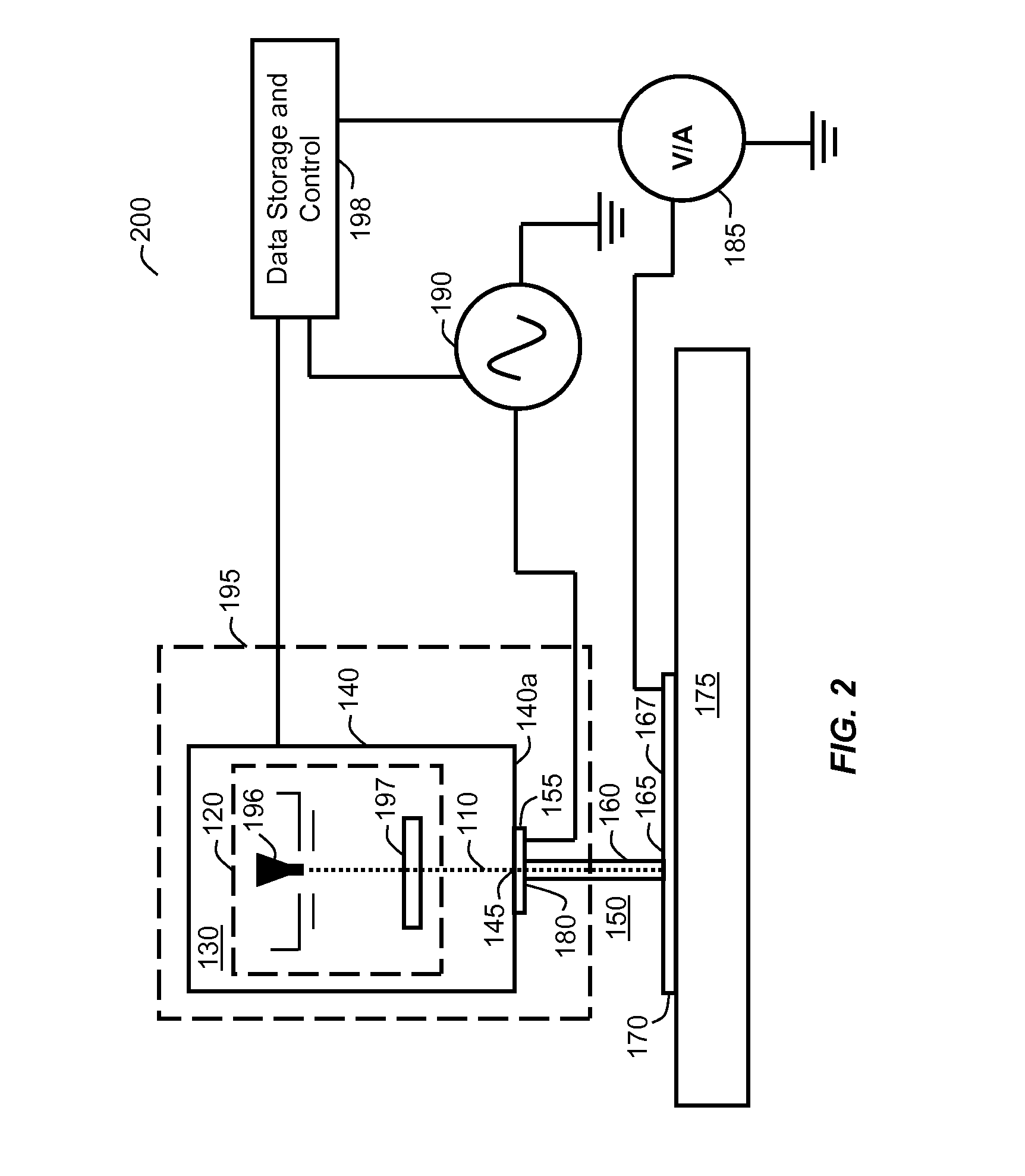
[0046]FIG. 2 is a schematic and cross sectional view of a non-mechanical contact signal measurement apparatus 200, in accordance with the present invention. The embodiment shown in FIG. 2 corresponds to the embodiment shown in FIG. 1 except in the embodiment shown in FIG. 2, electrical measurement device 185 is coupled to first conductor 165 and signal source 190 is coupled to second conductor 180. The other elements in FIG. 2 have the same functions as those in FIG. 1 with the same reference numbers and will not be described in detail again.

[0047]In order to determine suitable working conditions for the e-beam induced plasma probe method, simulations of the spatial and temporal distributions of the primary and secondary electrons as well as the ions involved in the process have been performed. FIG. 3 shows exemplary simulation data for plasma beam resistance, effective plasma beam resistance, electron beam energy, and plasma beam diameter associated with the non-mechanical contact ...


PUM


Abstract

A non-mechanical contact signal measurement apparatus includes a first conductor on a structure under test and a gas in contact with the first conductor. At least one electron beam is directed into the gas so as to induce a plasma in the gas where the electron beam passes through the gas. A second conductor is in electrical contact with the plasma. A signal source is coupled to an electrical measurement device through the first conductor, the plasma, and the second conductor when the plasma is directed on the first conductor. The electrical measurement device is responsive to the signal source.

Description

CROSS-REFERENCES TO RELATED APPLICATIONS[0001]This application claims priority to and is a continuation of PCT / US2012 / 046100, filed Jul. 10, 2012 and entitled “ELECTRICAL INSPECTION OF ELECTRONIC DEVICES USING ELECTRON-BEAM INDUCED PLASMA PROBES”, which claims the benefit under 35 U.S.C. §119(e) of U.S. provisional application No. 61 / 508,578, filed Jul. 15, 2011, entitled “ELECTRICAL INSPECTION OF ELECTRONIC DEVICES USING ELECTRON-BEAM INDUCED PLASMA PROBES”, the contents of which are incorporated herein by reference in their entirety.BACKGROUND[0002]The present invention relates generally to the non-mechanical contact probing of electronic devices and in particular, to the non-mechanical contact measurement of electronic signals during electrical inspection of electronic devices.[0003]The ability to measure and apply voltages and currents on patterned structures without having to establish mechanical contact is of importance to the functional (electrical) testing of semiconductor d...

Claims


Application Information

Patent Timeline
IPC IPC(8): G01R1/07
CPCG01R1/072G01R31/305H01J33/00H01J2237/164
Inventor KADYSHEVITCH, ALEXANDERKADAR, OFERGLAZER, ARIELOEWINGER, RONENGROSS, ABRAHAMTOET, DANIEL
Owner ORBOTECH LTD
Why Eureka
Try Eureka