Thin film transistor, TFT substrate and liquid crystal display unit

Active Publication Date: 2006-09-12
VISTA PEAK VENTURES LLC
View PDF6 Cites 5 Cited by
  • Summary
  • Abstract
  • Description
  • Claims
  • Application Information

AI Technical Summary

Benefits of technology

[0011]The present invention provides a liquid crystal display unit using a thin film transistor, a TFT substrate and a liquid crystal display unit which reduces light-induced leakage current of the thin film trans

Problems solved by technology

When light becomes incident on this active layer, leakage current (light-induced leakage current) due to optical excitation occurs so that the display performance

Method used


Image

  • Thin film transistor, TFT substrate and liquid crystal display unit
  • Thin film transistor, TFT substrate and liquid crystal display unit
  • Thin film transistor, TFT substrate and liquid crystal display unit

Examples


first embodiment

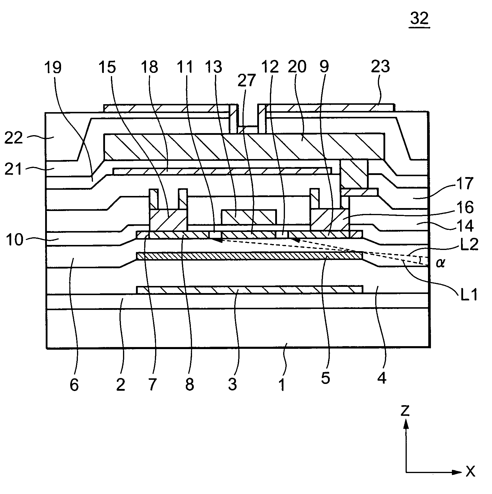
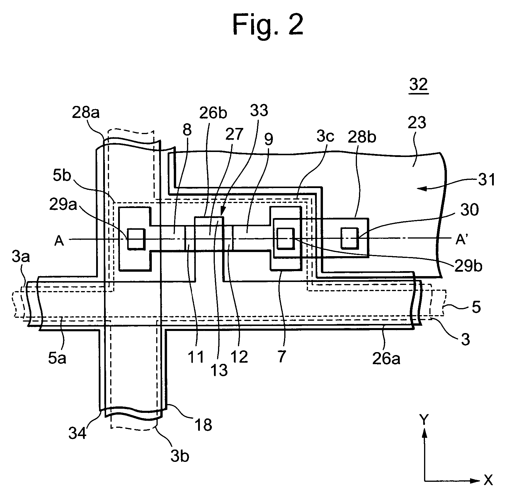
[0029]FIG. 2 is a plan view showing a thin film transistor of a liquid crystal display unit according to the present invention, and FIG. 3 is a cross-sectional view taken on line A–A′ of FIG. 2. In FIGS. 2 and 3, one of a plurality of thin film transistors to be contained in the TFT substrate 32 is shown.

[0030]As shown in FIG. 2, a TFT substrate 32 has a plurality of thin film transistors 33 to be arranged like a matrix shape, and each thin film transistor 33 is formed in the vicinity of intersections between a plurality of data lines 28a extending along a Y direction in parallel with each other and a plurality of gate lines 26a extending along an X direction in parallel with each other. The gate line 26a is made of, for example, polysilicon film or siliside film, in which carrier has been doped, and the data line 28a is made of aluminum film or the like. A black matrix 34 is made of chromium film or the like having light-shielding property, and is formed so as to spatially overlap ...

second embodiment

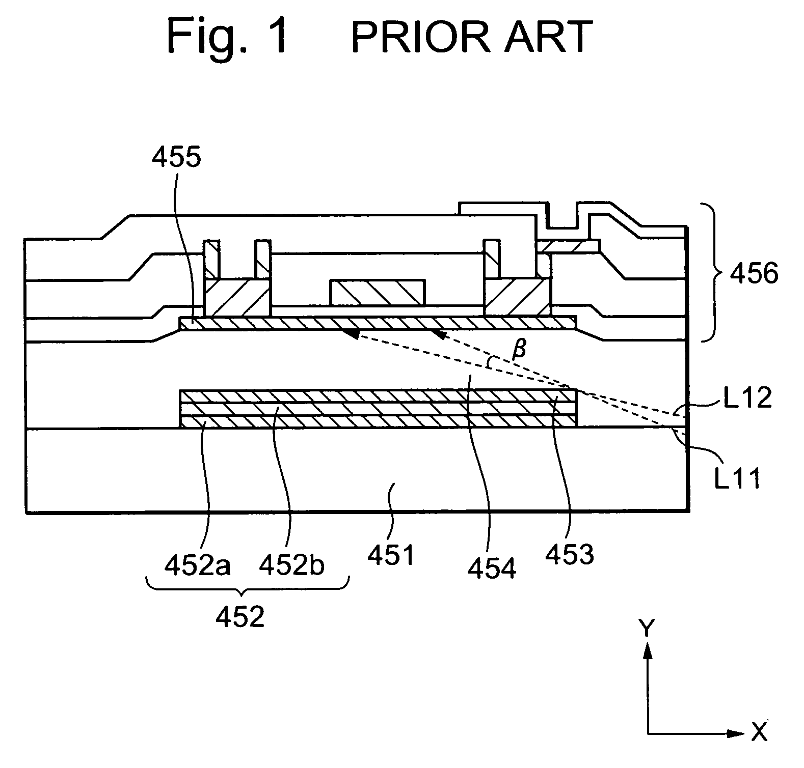
[0059]FIGS. 10(a) and (b) show a method of making the TFT substrate 32A of the present invention. First, by the CVD method, a ground dielectric film 2 is formed at a film thickness of about 300 nm on the entire surface on the substrate 1 made of, for example, high strain point glass substrate or the like. On the ground dielectric film 2, a tungsten siliside film, which is a metallic siliside film having a optical reflective property, is formed at a film thickness of about 175 nm as the first light-shielding film 3 by the sputtering method. Further, on the upper layer thereof, a second light-shielding film 5 is stacked at film thickness of about 60 nm by the CVD method (FIG. 10(a)).

[0060]Next, photo-resist is left behind in a region, in which the active layer 7 is formed, or in a region somewhat broader than it by the photolithography, and the second light-shielding film 5 is removed by the dry etching method (FIG. 10(b)). Subsequently to FIG. 10(b), by fabricating by the similar pro...

fifth embodiment

[0068]FIG. 13 shows cross-sectional structure of a TFT substrate 32D of a liquid crystal display unit according to the present invention. In this respect, FIG. 13 shows a process of forming the active layer 107 corresponding to an active layer 7 in FIG. 3. Also, the TFT substrate 32D is close to the pixel region 31 shown in FIG. 2, and the drain has a pixel matrix region 103, in which there is formed a thin film transistor for controlling a pixel to be connected to the pixel electrode, and a driving region 104, in which a peripheral circuit such as a driving circuit is formed.

[0069]The TFT substrate 32D having cross-sectional structure shown in FIG. 13 is obtained as below. First, as in the case of FIGS. 4(a) and (b), a ground dielectric film 102 is formed on the entire surface on a substrate 101 to form a light-shielding film 105 at a desired place. At this time; a light-shielding film 105 is formed in a pixel matrix region 103 but the light-shielding film 105 is not formed in a dr...


PUM


Abstract

A thin film transistor is provided including an active layer, in which a source region and drain region are formed, a first light-shielding film shielding a light incident on the active layer, and a second light-shielding film between the active layer and the first shielding film. A carrier concentration of at least surface portion of the second light-shielding film which opposes the active layer is about 1017/cm3 or less.

Description

BACKGROUND OF THE INVENTION[0001]1. Field of the Invention[0002]The present invention relates to a thin film transistor device, a liquid crystal display unit and a manufacturing method for the same, and more particularly, to a thin film transistor device and a liquid crystal display unit which reduces leakage current of a thin film transistor device.[0003]2. Description of the Related Art[0004]In recent years, as a display unit for OA (Office Automation) equipment, various display units using a liquid crystal display unit have been developed. Among various liquid crystal display units, an active matrix type liquid crystal display unit having a thin film transistor (TFT) used as a switching element, has an advantage over conventional displays in that contrast or response speed is not lower much even when the number of scanning lines is increased. For this reason, for high-grade display units for OA equipment and display units for high definition TVs, active matrix type liquid crystal...

Claims


Application Information

Patent Timeline
IPC IPC(8): H01L29/04G02F1/136G02F1/1335G02F1/1362G02F1/1368G09F9/30G09F9/35H01L21/77H01L21/84H01L27/12H01L29/786
CPCH01L29/78633H01L29/78621G02F1/136209H01L27/12H01L27/1214H01L27/1218
Inventor MATSUNAGA, NAOKISERA, KENJI
Owner VISTA PEAK VENTURES LLC
Why Eureka
Try Eureka