Image sensor

Pending Publication Date: 2022-07-07
SAMSUNG ELECTRONICS CO LTD
View PDF0 Cites 0 Cited by
  • Summary
  • Abstract
  • Description
  • Claims
  • Application Information

AI Technical Summary

Benefits of technology

[0004]Exemplary embodiments provide an image sensor that reduces light incident on internal device isolation film using an image

Problems solved by technology

However, a device isolation film in the pixel ar

Method used


Image

  • Image sensor
  • Image sensor
  • Image sensor

Examples


Embodiment Construction

[0016]Hereinafter, exemplary embodiments will be described with reference to the accompanying drawings.,

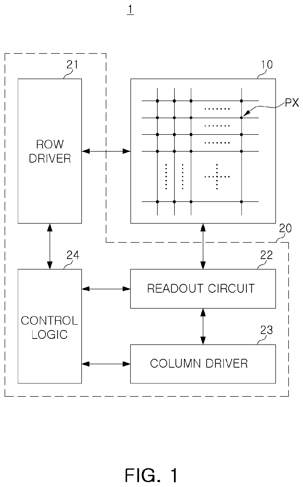
[0017]FIG. 1 is a block diagram of an image sensor according to an exemplary embodiment.

[0018]Referring to FIG. 1, an image sensor 1 according to an exemplary embodiment includes a pixel array 10 and a logic circuit 20.

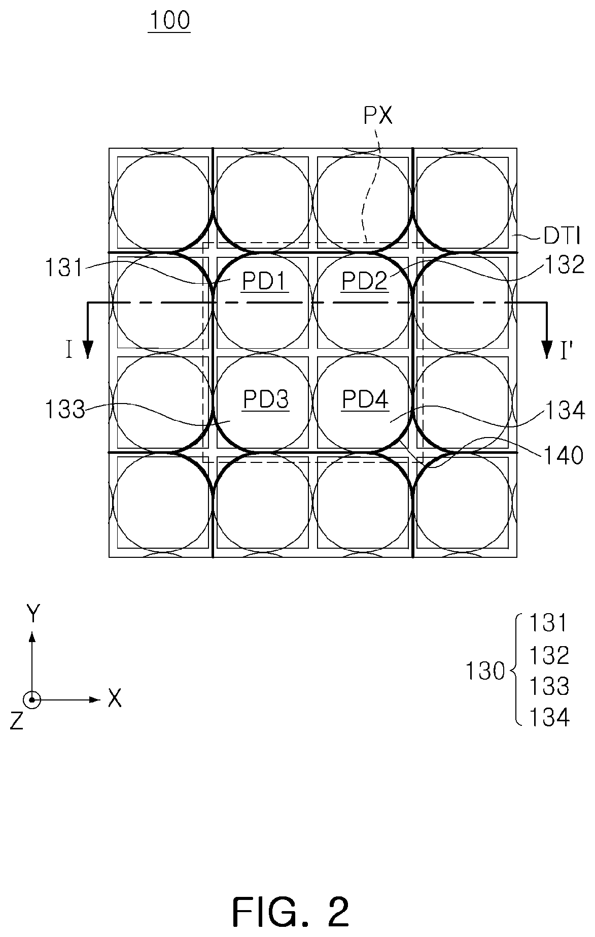
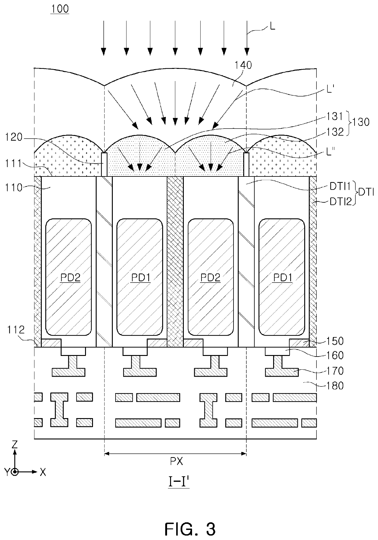
[0019]In an embodiment, the pixel array 10 includes a plurality of unit pixels PX disposed in an array in a plurality of rows and a plurality of columns. Each of the unit pixels PX includes at least one photoelectric conversion element that generates electric charges in response to light, and a pixel circuit that generates a pixel signal that corresponds to the electric charges generated by the photoelectric conversion element.

[0020]Then photoelectric conversion device includes a photodiode formed of a semiconductor material, and / or an organic photodiode formed of an organic material. In an exemplary embodiment, each of the unit pixels PX includes two or more photoe...


PUM


Abstract

An image sensor includes a substrate that includes first and second surfaces that oppose each other in a first direction and pixel areas arranged in directions parallel to the first surface, a first device isolation film that separates the pixel areas, four photodiodes disposed in each of the pixel areas inside of the substrate, and arranged in a 2×2 array, a second device isolation film that separates the four photodiodes from each other, a color filter disposed on the first surface of the substrate, and that includes four regions that respectively correspond to the four photodiodes, wherein each region has a convex upper surface, and a first microlens disposed above the color filter and that corresponds to each of the pixel areas. Accordingly, in the image sensor, light incident on the internal device isolation film is reduced, and loss of autofocusing sensitivity of the image sensor is reduced.

Description

CROSS-REFERENCE TO RJELAFED APPLICAIION(S)[0001]This application claims priority under 35 USC 119(a) from Korean Patent Application No. 10-2021-0000276, filed on Jan. 4, 2021 in the Korean Intellectual Property Office, the contents of which are herein incorporated by reference in their entirety.BACKGROUNDTechnical Field[0002]Embodiments of the present inventive concept are directed to an image sensor.Discussion of the Related Art[0003]I age sensors are semiconductor devices that convert optical images into electrical signals. Among such image sensors, a Complementary Metal Oxide Semiconductor (CMOS) type image sensor is abbreviated as a CMOS image Sensor (CIS). A CIS includes a plurality of pixel areas, and each of the pixel areas includes at least one photodiode (PD) that converts incident light into an electrical signal. On the other hand, a CIS that includes tour photodiodes in one pixel area can have improved autofocusing performance. However, a device isolation film in the pixe...

Claims


Application Information

Patent Timeline
IPC IPC(8): H01L27/146H04N5/369
CPCH01L27/14621H04N5/36961H01L27/14685H01L27/14627H01L27/1463H01L27/14645H01L27/14643H01L27/14605H04N25/704H04N25/134H01L27/1461
Inventor LEE, SEUNGWOOKKIM, MIHYELEE, HAEWON
Owner SAMSUNG ELECTRONICS CO LTD
Why Eureka
Try Eureka