Semiconductor memory device and refresh period controlling method

a memory device and memory technology, applied in the field of semiconductor memory devices, can solve the problems of inability to produce, lack of circuit design techniques, and difficulty in achieving extensive temperature traceability circuit design, and achieve stable temperature adjustment, reduce cost, and improve temperature compensation characteristics.

Inactive Publication Date: 2009-02-17
PS4 LUXCO SARL
View PDF26 Cites 65 Cited by
  • Summary
  • Abstract
  • Description
  • Claims
  • Application Information

AI Technical Summary

Benefits of technology

[0033]Accordingly, it is an object of the present invention to provide a semiconductor memory device and a refresh period controlling method in which there is exploited a temperature compensation technique whereby marked reduction in the data retention current may be achieved.
[0055]According to the present invention, the memory cells, in which the expected value data have been written, are read with a period equal to or shorter than a refresh period, and compared with the expected value data to measure an error count or an error rate, and in which the refresh period is variably controlled based on the measured results, so that temperature compensation characteristics may be improved appreciably.
[0056]Moreover, according to the present invention, the trimming adjustment in the manufacture process may be dispensed with to reduce the cost, while stable temperature adjustment may be achieved extremely readily.

Problems solved by technology

It is however technically difficult to design a circuit showing extensive temperature traceability suited to a device, such that there lacks an efficacious circuit designing technique.
This poses a serious problem in a wafer test step (the step of applying a probe on a pad of a wafer chip to carry out an electrical test of a die).
As a result, fails tend to be produced at a mid temperature range so that a large operating margin needs to be provided as the variations are taken into account.
With the result that it is not possible to achieve marked temperature traceability.

Method used


Image

  • Semiconductor memory device and refresh period controlling method
  • Semiconductor memory device and refresh period controlling method
  • Semiconductor memory device and refresh period controlling method

Examples


embodiment

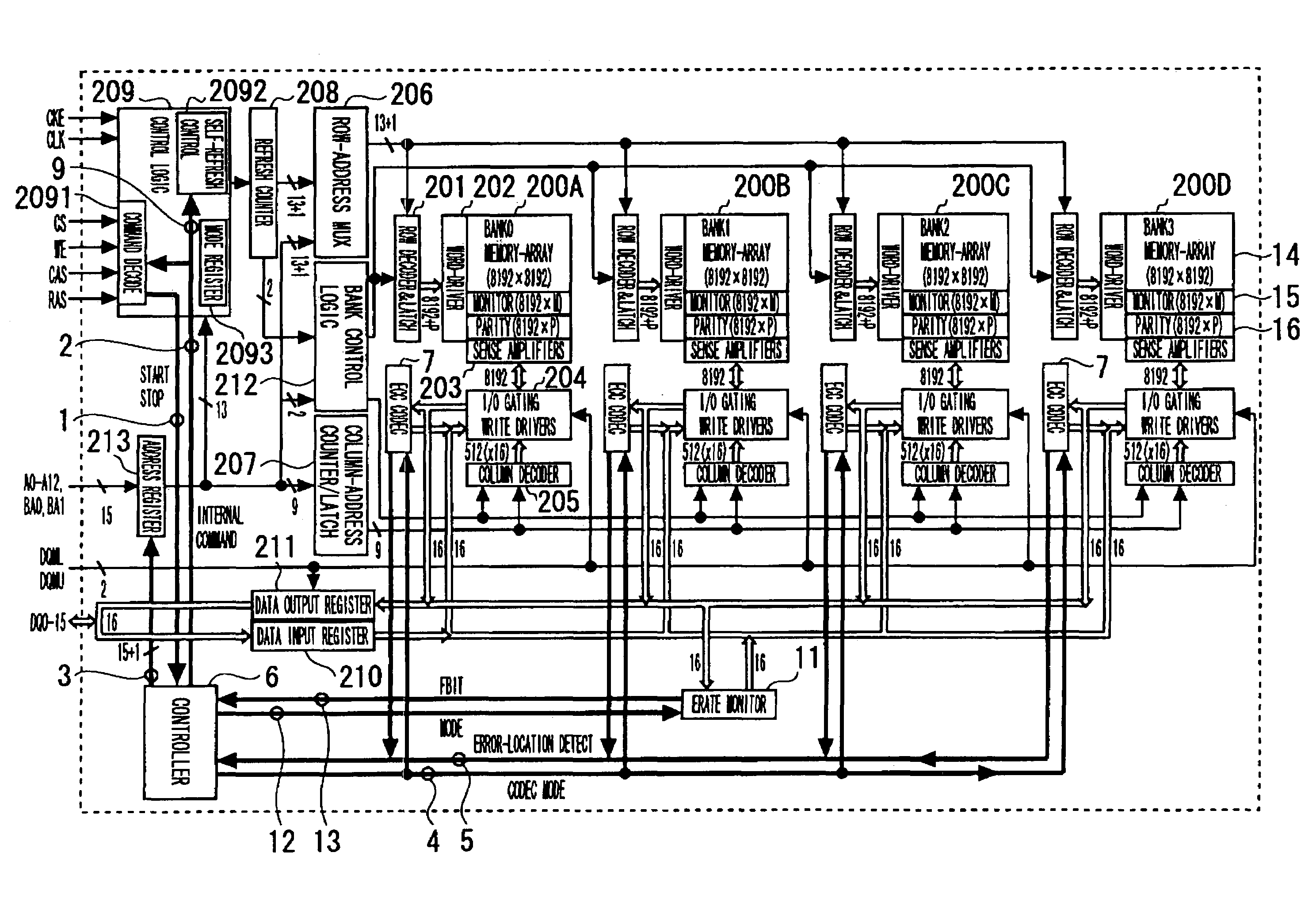
[0157]FIG. 5 is a diagram showing the configuration of a semiconductor memory device according to an embodiment of the present invention. FIG. 5 depicts an overall block diagram of an embodiment of a dynamic RAM (referred to below simply as DRAM) of the present invention. The DRAM of the present embodiment is an SDRAM (synchronous dynamic random-access memory). The SDRAM of the present embodiment has four memory arrays 200A to 200D in association with four memory banks (BANK 0 to 3). The memory arrays 200A to 200D, associated with the four memory banks 0 to 3 (BANK 0 to 3), are each provided with a matrix array of dynamic memory cells. In each memory array of FIG. 5, the gate terminal of a memory cell transistor, not shown, is connected to a word line, not shown, for providing on / off control of the memory cell transistor. One of the drain and the source of the memory cell transistor connected to a bit line, not shown, complementary from row to row, with the other of the drain and th...


PUM


Abstract

Disclosed is a memory device including an error rate measurement circuit and a control circuit. The error rate measurement circuit, carrying a BIST circuit, reads out and writes data for an area for monitor bits every refresh period to detect an error rate (error count) with the refresh period. The control circuit performs control for elongating and shortening the refresh period so that a desired error rate will be achieved. The BIST circuit issues an internal command and an internal address and drives the DRAM from inside. The BIST circuit writes and reads out desired data, compares the monitor bits to expected values (error decision) and counts the errors.

Description

FIELD OF THE INVENTION[0001]This invention relates to a semiconductor memory device and, more particularly, to a semiconductor memory device in need of refresh for data retention, and to a refresh period controlling method.BACKGROUND OF THE INVENTION[0002]Capability of pause refresh of a memory device is widely changed responsive to ambient temperature. Temperature compensation of a self-refresh period is the technique of controlling the refresh period for coping with the temperature dependency of the capability of pause refresh. If the technique of temperature compensation of the self-refresh period is brought to completion, it is possible to reduce the data retention current by one order of magnitude at ambient temperature as compared with that at elevated temperatures (upper limit of the guaranteed temperature). It is however technically difficult to design a circuit showing extensive temperature traceability suited to a device, such that there lacks an efficacious circuit design...

Claims


Application Information

Patent Timeline
Patent Type & Authority Patents(United States)
IPC IPC(8): G06F11/00H03M13/00G11C7/00G11C11/406
CPCG11C11/406G11C2211/4061G11C2211/4062G11C11/4096
Inventor ITO, YUTAKAHASHIMOTO, TAKESHI
Owner PS4 LUXCO SARL
Why Eureka
Try Eureka