
Electro-optical device and electronic apparatus

a technology of optical devices and electronic devices, applied in the direction of static indicating devices, identification means, instruments, etc., can solve the problems of inefficient incident of light on the intrinsic layer, increased man-hours and costs, and inability to efficiently generate photogenerated charges, etc., to achieve efficient incident and sufficient light sensitivity

Active Publication Date: 2009-03-03
JAPAN DISPLAY WEST
View PDF17 Cites 5 Cited by
  • Summary
  • Abstract
  • Description
  • Claims
  • Application Information

AI Technical Summary

Benefits of technology

"The invention is about an electro-optical device and an electronic apparatus that can detect light with high sensitivity. The device includes an insulating substrate, a switching element, at least one PIN diode, and at least one reflector. The reflector is formed in the same layer as the gate electrode and opposite the PIN diode, and can reflect light incident on the insulating substrate. This allows most of the light to be incident on the PIN diode, and the ambient light can be detected with high sensitivity. The reflector is connected to a fixed potential point, which prevents it from affecting the characteristics of the PIN diode. The electronic apparatus includes the electro-optical device and an illuminating unit for blocking the light from the illuminating unit from being incident on the PIN diode. This allows accurate detection of ambient light."

Problems solved by technology

This increases the man-hour and the cost.
However, in the case where the semiconductor layer in the PIN diode forming region is thin, incident light passes through the semiconductor layer, and photogenerated charges cannot be efficiently generated.
That is to say, light is not efficiently incident on the intrinsic layer, and a sufficient light sensitivity cannot be obtained.

Method used


Image

  • Electro-optical device and electronic apparatus
  • Electro-optical device and electronic apparatus
  • Electro-optical device and electronic apparatus

Examples


first exemplary embodiment

[0035]First, the overall structure of the electro-optical device according to the first exemplary embodiment will be described with reference to FIGS. 2 to 4.

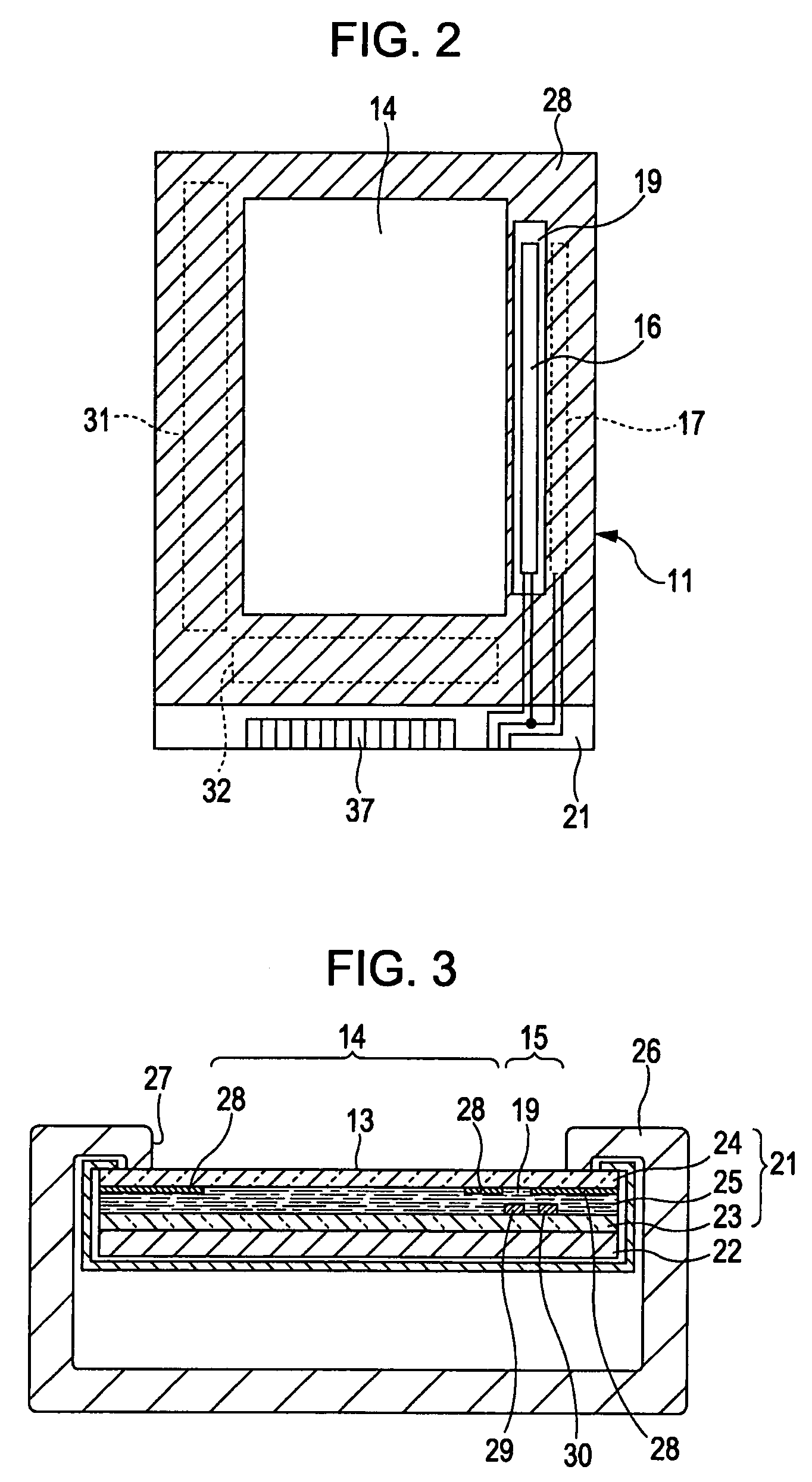
[0036]In FIG. 2, the electro-optical device 11 includes a display panel 21 including two substrates stuck together. In the case of FIG. 3, a liquid crystal panel is employed as the display panel 21. In this case, the electro-optical device 11 includes the display panel 21 and an illuminating unit 22. A self-luminous display panel can also be employed as the electro-optical device. In this case, no illuminating unit is necessary.

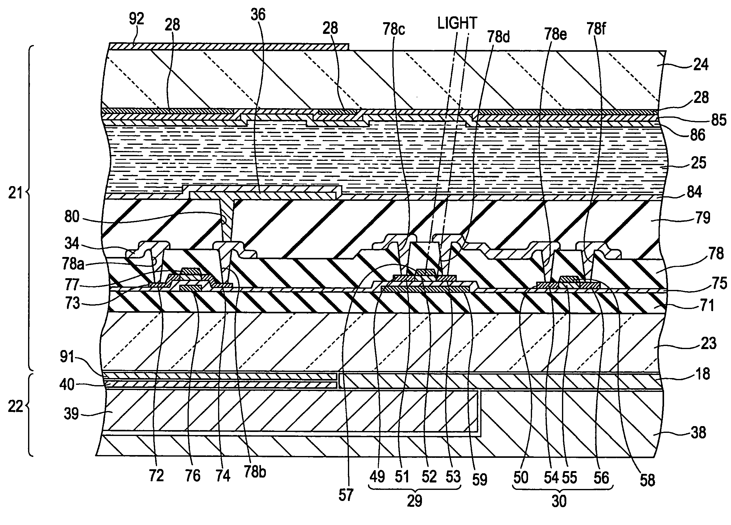
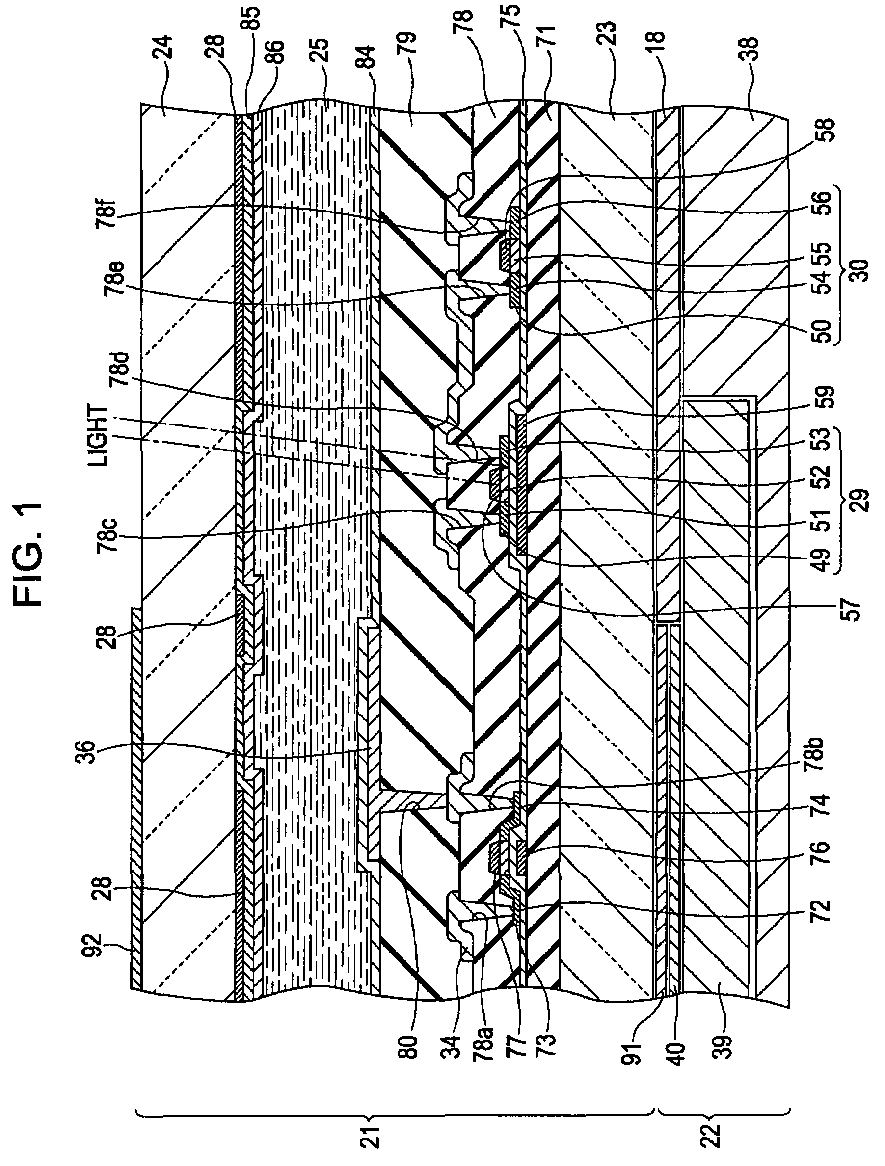
[0037]As shown in FIG. 3, the display panel 21 includes a light-transmitting element substrate 23, a light-transmitting opposing substrate 24, and liquid crystal 25 enclosed therebetween. The element substrate 23 and the opposing substrate 24 facing each other are stuck together with a sealing material (not shown). The display panel 21 includes, for example, a plurality of scanning lines 33 extending in ...

second exemplary embodiment

[0082]FIG. 6 is a perspective view schematically showing the electro-optical device according to a second exemplary embodiment of the invention. In FIG. 6, the same reference numerals will be used to designate the same components as those in FIG. 1, so that the description will be omitted.

[0083]The reflectors 59 in the first exemplary embodiment are formed of metal and are in a floating status. Therefore, an unforeseen parasitic capacity is generated between the cathode (N-type region 51) of each PIN diode 29 and the corresponding reflector 59 and between the anode (P-type region 53) of each PIN diode 29 and the corresponding reflector 59. In addition, the reflectors 59 can be charged with static electricity. In this case, the electrical impact due to the reflectors 59 is brought on the anodes and cathodes of the PIN diodes 29. In this case, by extending each reflector 59 up to under the corresponding anode and up to under the corresponding cathode in the same manner, the electrical...


PUM

PropertyMeasurementUnit
luminanceaaaaaaaaaa
semiconductoraaaaaaaaaa
brightnessaaaaaaaaaa

Abstract

An electro-optical device includes an insulating substrate, a switching element, at least one PIN diode, and at least one reflector. The switching element includes a first polysilicon semiconductor layer formed on the insulating substrate, and a gate electrode formed between the insulating substrate and the first semiconductor layer. Each of the at least one PIN diode includes a second polysilicon semiconductor layer formed on the insulating substrate. The at least one reflector is formed in the same layer as the gate electrode and opposite the second semiconductor layer or layers of the at least one PIN diode.

Description

BACKGROUND[0001]1. Technical Field[0002]The present invention relates to electro-optical devices and electronic apparatuses suitable for display devices that control their display luminances.[0003]2. Related Art[0004]A liquid crystal panel includes two substrates, such as glass substrates or quartz substrates, and liquid crystal filled therebetween. The substrates are provided with electrodes, and image signals are supplied to the electrodes. The optical characteristic of the liquid crystal between the electrodes of the substrates changes according to the image signals. That is to say, by applying voltages based on the image signals to the liquid crystal between the electrodes of the substrates, the alignment of liquid crystal molecules is changed. Thus, the light transmittance in each pixel changes according to the image signals, and an image display according to the image signals is performed.[0005]In order to perform a high-luminance display in such a liquid crystal panel, in gen...

Claims


Application Information

Patent Timeline
Patent Type & Authority Patents(United States)
IPC IPC(8): H01L33/00G02F1/133G02F1/13357G02F1/1362G02F1/1368G09F9/30H01L21/336H01L29/786
CPCG02F1/13318G02F1/1362
Inventor KOIDE, SHINMURAMATSU, HIROKOFUJITA, SHIN
Owner JAPAN DISPLAY WEST
Learn More