Liquid crystal display device and method for manufacturing the same

a technology of liquid crystal display and liquid crystal, which is applied in the direction of photosensitive materials, instruments, photomechanical equipment, etc., can solve the problems of poor adhesion to the substrate, peeling off from the substrate, and uneven distribution of spacers, so as to reduce the generation of process errors, improve the reliability of the device, and reduce the effect of process time and cos

Active Publication Date: 2009-03-10
LG DISPLAY CO LTD
View PDF1 Cites 13 Cited by
  • Summary
  • Abstract
  • Description
  • Claims
  • Application Information

AI Technical Summary

Benefits of technology

[0023]An advantage of the present invention is to provide a liquid crystal display (LCD) device having a polymer adhesive layer interposed between a substrate and a pattern and / or between one pattern and another pattern, and a method for manufacturing the same. The polymer adhesive layer reduces the generation of process errors and improves reliability of the device.
[0024]Another advantage of the present invention is to provide a liquid crystal display (LCD) device having a polymer adhesive layer formed by an easy method, such as a spin coating method or an ink-jet printing method, and a method for manufacturing the same.
[0025]Another advantage of the present invention is to provide a liquid crystal display (LCD) device having a polymer adhesive layer that is formed by a method that does not require a photo-etching process, and a method for manufacturing the same. Thus, process time and costs are not increased.

Problems solved by technology

First, a metal material, which is used to form the gate lines, has poor adhesion to the substrate and thus peels off from the substrate.
Second, when the cell gap between the bonded substrates increases due to various reasons, the spacers for maintaining the cell gap between the bonded substrates are not fixed in the liquid crystal layer and are movable in the liquid crystal layer. Thus, the spacers may not be uniformly distributed, and when the liquid crystal display device is moved, the spacers gather due to gravity.
Third, when the overcoat layer is formed on the overall surface of the substrate including the color filter layers, the overcoat layer may peel off from the edge of the substrate having the sealant formed thereon. To solve the above problems in the related art, a patterning process for removing the overcoat layer from the edge of the substrate is additionally performed. However, in this related art patterning process, a photo-etching process and an expensive exposure apparatus are additionally required. Thus, process time and costs are increased.

Method used


Image

  • Liquid crystal display device and method for manufacturing the same
  • Liquid crystal display device and method for manufacturing the same
  • Liquid crystal display device and method for manufacturing the same

Examples


first embodiment

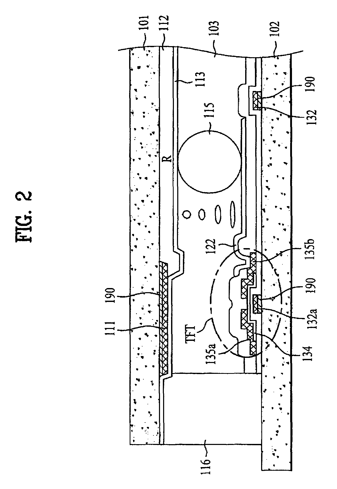
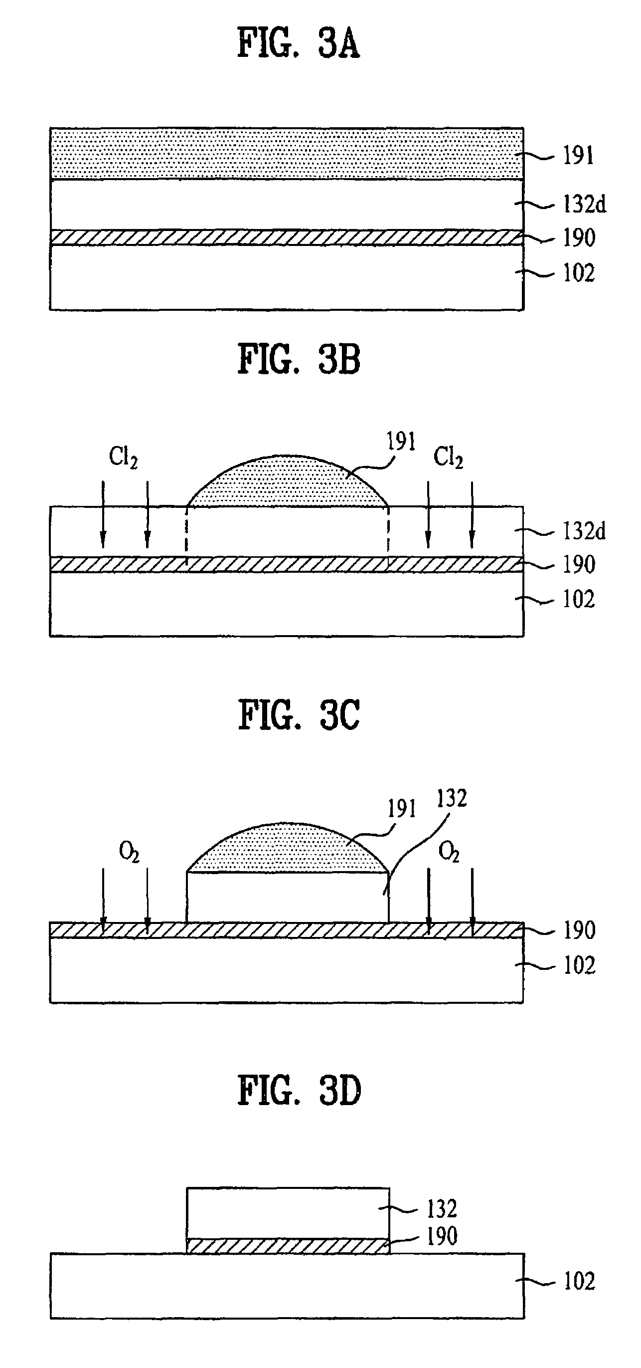
[0039]FIG. 2 is a sectional view of a liquid crystal display device in accordance with a first embodiment of the present invention, and FIGS. 3A to 3D are sectional views illustrating a method for manufacturing the liquid crystal display device in accordance with the first embodiment of the present invention.

[0040]As shown in FIG. 2, the liquid crystal display device of the first embodiment includes first and second substrates 102 and 101 opposing each other, a sealant 116 that bonds the first and second substrates 102 and 101 to each other deposited along the edge of the first substrate 102 except for a liquid crystal inlet, spacers 115 that maintain a cell gap between the first and second substrates 102 and 101 and a cell gap at the liquid crystal inlet, and a liquid crystal layer 103 filling a space between the first and second substrates 102 and 101.

[0041]Data lines (not shown) and gate lines 132 that cross each other to define sub-pixels and TFTs formed at the crossings between...

second embodiment

[0055]FIG. 4 is a sectional view of a liquid crystal display device in accordance with a second embodiment of the present invention, and FIGS. 5A to 5D are sectional views illustrating a method for manufacturing the liquid crystal display device in accordance with the second embodiment of the present invention.

[0056]As shown in FIG. 4, the liquid crystal display device of the second embodiment includes first and second substrates 202 and 201 opposing each other, a sealant 216 that bonds the first and second substrates 202 and 201 to each other deposited along the edge of the first substrate 202 except for a liquid crystal inlet, spacers 215 that maintain a cell gap between the first and second substrates 202 and 201 and a cell gap at the liquid crystal inlet, and a liquid crystal layer 203 filling a space between the first and second substrates 202 and 201.

[0057]Data lines (not shown) and gate lines 232 that cross each other to define sub-pixels and TFTs formed at the crossings betw...

third embodiment

[0072]FIG. 6 is a sectional view of a liquid crystal display device in accordance with a third embodiment of the present invention and FIG. 7 is a sectional view illustrating a method for manufacturing the liquid crystal display device in accordance with the third embodiment of the present invention.

[0073]As shown in FIG. 6, the liquid crystal display device of the third embodiment includes first and second substrates 302 and 301 opposing each other, a sealant 316 that bonds the first and second substrates 302 and 301 to each other deposited along the edge of the first substrate 302 except for a liquid crystal inlet, spacers 315 that maintain a cell gap between the first and second substrates 302 and 301 and a cell gap at the liquid crystal inlet, a polymer adhesive layer 391 interposed between the spacers 315 and a pattern of the second substrate 301, and a liquid crystal layer 303 filling a space between the first and second substrates 302 and 301.

[0074]Because the spacers 315 are...


PUM

PropertyMeasurementUnit
thicknessaaaaaaaaaa
sizeaaaaaaaaaa
temperatureaaaaaaaaaa

Abstract

A liquid crystal display device having a polymer adhesive layer interposed between a substrate and a pattern or between one pattern and another pattern, and a method for manufacturing the same are disclosed. The polymer adhesive layer is interposed where peeling problems occur. The polymer adhesive layer reduces process errors and improves reliability. The device includes: a first substrate; gate lines, data lines, TFTs, and pixel electrodes on a surface of the first substrate; a second substrate bonded to the first substrate; a liquid crystal layer between the first and second substrates; a black matrix layer and a color filter layer on a surface of the second substrate; a sealant formed along an edge of a substrate that bonds the first and second substrates to each other; spacers that maintain a cell gap between the first and second substrates; and a polymer adhesive layer that improves adhesive characteristics.

Description

[0001]This application claims the benefit of Korean Patent Application 10-2005-0114268, filed on Nov. 28, 2005, which is hereby incorporated by reference for all purposes as if fully set forth herein.BACKGROUND OF THE INVENTION[0002]1. Field of the Invention[0003]The present invention relates to a liquid crystal display device and a method for manufacturing the same. More particularly, the present invention relates to a liquid crystal display device having a nano-polymer adhesive layer that prevents a peeling problem from occurring between a substrate and a pattern and / or between one pattern and another pattern, and a method for manufacturing the same.[0004]2. Discussion of the Related Art[0005]New high-tech visual display devices, such as high definition TVs are currently being developed. Accordingly, flat panel display devices have been developed to replace cathode ray tubes (CRT). The flat panel display devices include liquid crystal display (LCD) devices, electro luminescence di...

Claims


Application Information

Patent Timeline
Patent Type & Authority Patents(United States)
IPC IPC(8): C09K19/00C09K19/52
CPCG02F1/133711G02F1/13392G02F1/136286G02F1/13394Y10T428/1059G02F2202/022G02F2202/28Y10T428/10Y10T428/1005G02F2001/136295C09K2323/00C09K2323/02C09K2323/05G02F1/136295G02F1/1339
Inventor KIM, SOOPOOL
Owner LG DISPLAY CO LTD
Why Eureka
Try Eureka