Integrated optical semiconductor device

a semiconductor device and integrated technology, applied in semiconductor lasers, laser details, electrical apparatus, etc., can solve the problems of inefficiency of optical modulation, inability to use selective etching using tartaric acid, and inability to carry out non-selective etching, etc., to achieve good controllability and high efficiency of operation

Inactive Publication Date: 2009-03-10
MITSUBISHI ELECTRIC CORP
View PDF4 Cites 2 Cited by
  • Summary
  • Abstract
  • Description
  • Claims
  • Application Information

AI Technical Summary

Benefits of technology

[0026]The present invention has been made to solve the problem, and a first object thereof is to configure an integrated optical semiconductor device which is highly efficient in operation and low-cost and has three or more optical elements opposed and joined in the optical axis direction. A second object thereof is to provide a manufacturing method for integrating the integrated optical semiconductor device having the three or more kinds of optical elements opposed and joined in the optical axis direction with good controllability.
[0028]Accordingly, in the integrated optical semiconductor device according to the present invention, the deviations are reduced between the optical axis of the third optical semiconductor element structure and the optical axes of first and second optical semiconductor element structures. As losses due to the deviations of the optical axis are reduced, it is possible to obtain the integrated optical semiconductor device of a simple configuration, low cost and high operation efficiency.
[0030]Accordingly, in the manufacturing method of the integrated optical semiconductor device according to the present invention, in its etching process in the case of forming the third optical semiconductor element structure, it is possible, by forming the inter-optical semiconductor element structure, to perform the nonselective etching and the selective etching following the nonselective etching with the second mask pattern as the etching mask as with the etching in the process of forming the second optical semiconductor element structure so as to accurately control the etching depth. For this reason, the third optical semiconductor element structure formed by performing the embedding growth with the second mask pattern as the mask is formed with reduced position errors in the thickness direction thereof. And the deviations are reduced between the optical axis of the third optical semiconductor element structure and the optical axes of first and second optical semiconductor element structures located in front and in rear of the third optical semiconductor element structure. In addition, the yield is improved. Therefore, the losses due to the deviation of the optical axis are reduced as to the integrated optical semiconductor device according to this manufacturing method, and so it is possible to obtain the integrated optical semiconductor device of a simple configuration, low cost and high operation efficiency.

Problems solved by technology

Therefore, it is not possible to carry out the nonselective etching as performed on forming the window layer structure portion, which is performed by the selective etching, thereby to stop the etching with high-precision etching depth control.
However, it is not possible to use the selective etching using the tartaric acid to a part of the basic laminated structure of the window layer structure portion because it has the InP layer formed by the epitaxial growth existing on the InP substrate.
As regards the optical modulator integrated semiconductor laser device for instance, there arises a situation where a deviation occurs between an active layer of the semiconductor laser and an absorbing layer of the optical modulator so that optical modulation is not efficiently performed.
Thus, the conventional manufacturing method had a problem that, in the case of monolithically forming three or more optical elements having different double hetero basic laminated structures by the butt-joint, it was difficult to integrate optical semiconductor elements without the deviations of the relative positions in a layer thickness direction from the substrate with good controllability.

Method used


Image

  • Integrated optical semiconductor device
  • Integrated optical semiconductor device
  • Integrated optical semiconductor device

Examples


first embodiment

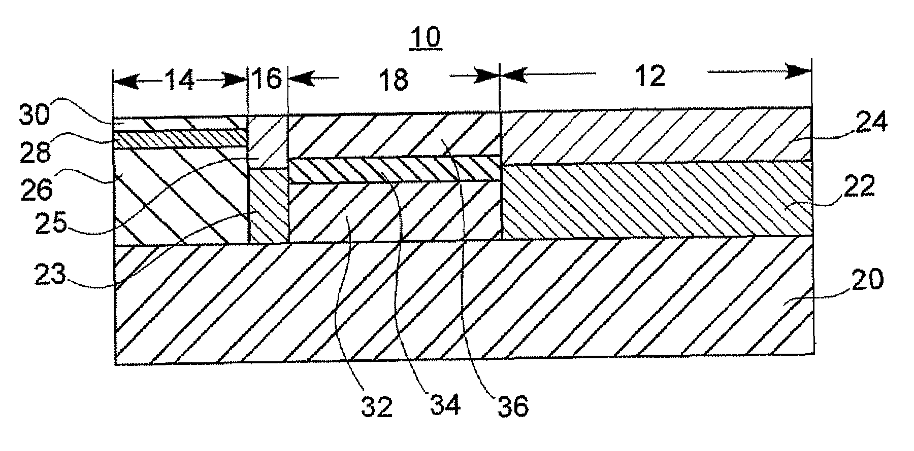
[0045]FIG. 1 is a sectional view showing a basic laminated structure of an integrated optical semiconductor device according to an embodiment of the present invention. In the following drawings, the same symbols represent the same or equivalent articles.

[0046]The sectional view of a basic laminated structure 10 of the integrated optical semiconductor device of FIG. 1 is the sectional view of a section parallel to a waveguide direction of a semiconductor laser.

[0047]The basic laminated structure 10 is configured as a basic laminated structure consisting of a semiconductor laser portion 12 as a first optical semiconductor element structure, a window layer structure portion 14 as a second optical semiconductor element structure located at the most front end in a light emitting direction of the basic laminated structure 10, a first inter-element portion 16 as an inter-optical semiconductor element structure in close contact with the window layer structure portion 14, a pre-placed optica...

second embodiment

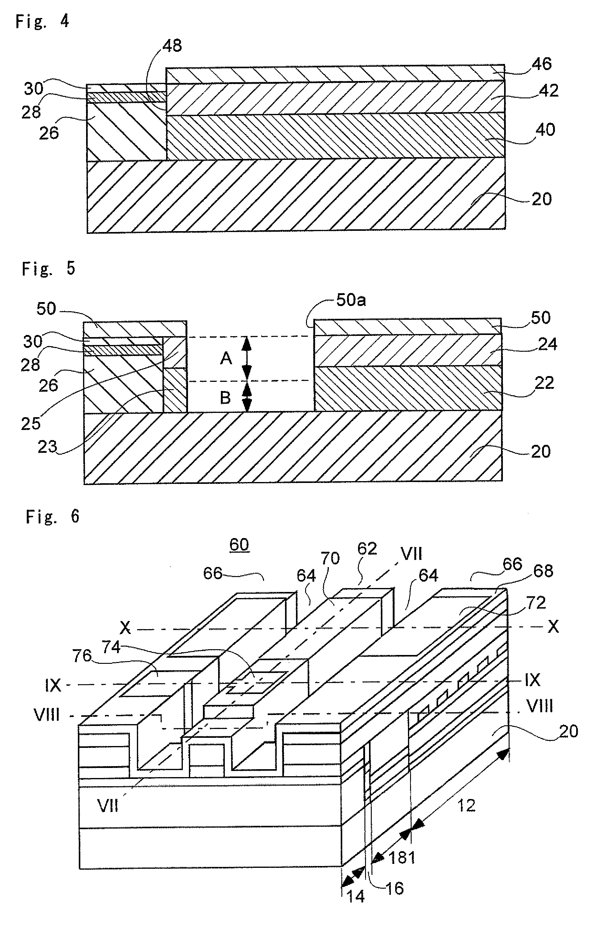
[0076]FIG. 6 is a perspective view of the integrated optical semiconductor device according to an embodiment of the present invention.

[0077]In FIG. 6, an optical modulator integrated semiconductor laser device 60 as the integrated optical semiconductor device is configured by the semiconductor laser portion 12, the window layer structure portion 14 located at the most front end in the light emitting direction, the first inter-element portion 16 in close contact with the window layer structure portion 14, and the pre-placed optical element portion 18 having the end face on its light emitting side in close contact with the first inter-element portion 16 and the end face on its light input side in close contact with the emitting end face of the semiconductor laser portion 12, that is, an optical modulator 181 according to the second embodiment.

[0078]The optical modulator integrated semiconductor laser device 60 has an optical element ridge portion 62 formed like a ridge in a central po...


PUM


Abstract

A semiconductor laser device includes a semiconductor laser portion, a window layer structure portion, a first inter-element portion, and a pre-placed optical element portion on an InP substrate. The semiconductor laser portion includes an InGaAsP layer and an InP layer located on the InGaAsP layer. The window layer structure portion of a double heterojunction structure has the same optical axis direction as the semiconductor laser portion and is located apart from the semiconductor laser portion. The first inter-element portion has a 100-μm or less thickness in an optical axis direction, is in contact with an end face on a side of the window layer structure portion adjacent to the semiconductor laser portion and includes an InGaAsP layer and an InP layer of the same layer configuration as the semiconductor laser portion. The pre-placed optical element portion of the double heterojunction structure has a first end face in contact with the first inter-element portion and a second end face mutually opposed to the first end face and in contact with one end face of the semiconductor laser portion.

Description

BACKGROUND OF THE INVENTION[0001]1. Field of the Invention[0002]The present invention relates to an integrated optical semiconductor device and a manufacturing method thereof, and particularly to an integrated optical semiconductor device monolithically formed by opposing and joining three or more kinds of optical elements in an optical axis direction and a manufacturing method thereof.[0003]2. Description of the Related Art[0004]In recent years, there is increasing demand for transmitting vast amounts of information at low cost as broadband communications makes progress and a public telecommunication network using an optical fiber prevails. To increase the amounts of information transmitted according to such demand, it is necessary to improve a transmission rate. The transmission rate is gradually sped up from 600 Mbps to 2.5 Gbps and further to 10 Gbps.[0005]Due to such improvement in the transmission rate of optical communication devices, optical communication networks expanded t...

Claims


Application Information

Patent Timeline
Patent Type & Authority Patents(United States)
IPC IPC(8): H01S5/00
CPCH01S5/026
Inventor MIYAZAKI, YASUNORI
Owner MITSUBISHI ELECTRIC CORP
Why Eureka
Try Eureka