Apparatus and methods for constructing balanced chip packages to reduce thermally induced mechanical strain

a technology of balanced chip and packaging, applied in the direction of printed circuit stress/warp reduction, printed circuit aspects, laminated printed circuit boards, etc., can solve the problems of device failure and structural defects, inability to implement electronic modules with increased chip densities and system performance, and more packaging problems, so as to prevent structural damage to chip package structures, reduce bowing, and in-plain strain

Inactive Publication Date: 2009-03-17
GLOBALFOUNDRIES INC
View PDF15 Cites 6 Cited by
  • Summary
  • Abstract
  • Description
  • Claims
  • Application Information

AI Technical Summary

Benefits of technology

[0013]Exemplary embodiments of the invention generally include apparatus and methods for constructing balanced semiconductor chip package structures that minimize bowing, in-plain strain and / or other thermally induced mechanical strains that may arise during thermal cycling, to thus prevent structural damage to chip package structures.
[0015]In one exemplary embodiment, the first stiffener plate is formed with a material and dimensioned to provide mechanical stability and planarity to the second substrate. The second stiffener plate is formed with a material and dimensioned to provide a mechanically balanced stacked structure above and below the region of the second substrate in the footprint areas where the IC chip to first carrier substrate assembly is attached to the second substrate.
[0016]For instance, in one exemplary embodiment of the invention, the first substrate and second stiffener plate are formed of silicon and the second substrate is an organic substrate (e.g., PCB, PWB). The package structure provides a balanced structure such that the organic substrate is in a neutral plane (i.e., there is no local bending in the organic substrate or in a SOP structure (Si chip on silicon carrier), and such that the in-plane expansion of the organic substrate is constrained so as to reduce shear strain in the interface between the organic substrate and chip carrier. For instance, a balanced structure can be obtained by selecting the material and dimensions of the second stiffener plate such that the second stiffener plate is formed of a material having a CTE similar to the chip carrier substrate and such that the second stiffener plate has a thickness that is matched to the effective stiffness of the SOP structure.

Problems solved by technology

The ability to implement electronic modules with increased chip densities and system performance is limited primarily by the ability to effectively remove heat from such electronic modules as resulting increased heat densities makes packaging more problematic.
Indeed, substantial stresses and strains may be generated in a package structure caused by thermal cycling during chip operation, leading to device failure and structural defects.
During thermal cycling, relative displacement between components due to differences in CTE between such components can cause bowing or bending of substrates and generate significant stresses and strains in the electrical contacts and interface between the components.
These stresses are applied repeatedly with repeated operation of the device, and can cause fatigue of the electrical interconnections, especially C4s.
In addition, the bending of the chip carrier (102) can cause undue stresses and strains between the chip carrier (102) and chip (101) leading to defects and structural damage, etc.

Method used


Image

  • Apparatus and methods for constructing balanced chip packages to reduce thermally induced mechanical strain
  • Apparatus and methods for constructing balanced chip packages to reduce thermally induced mechanical strain
  • Apparatus and methods for constructing balanced chip packages to reduce thermally induced mechanical strain

Examples


Embodiment Construction

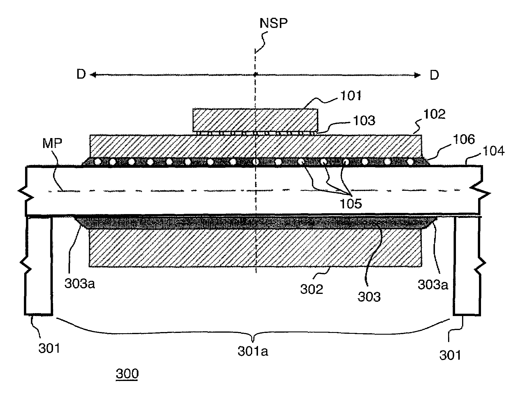
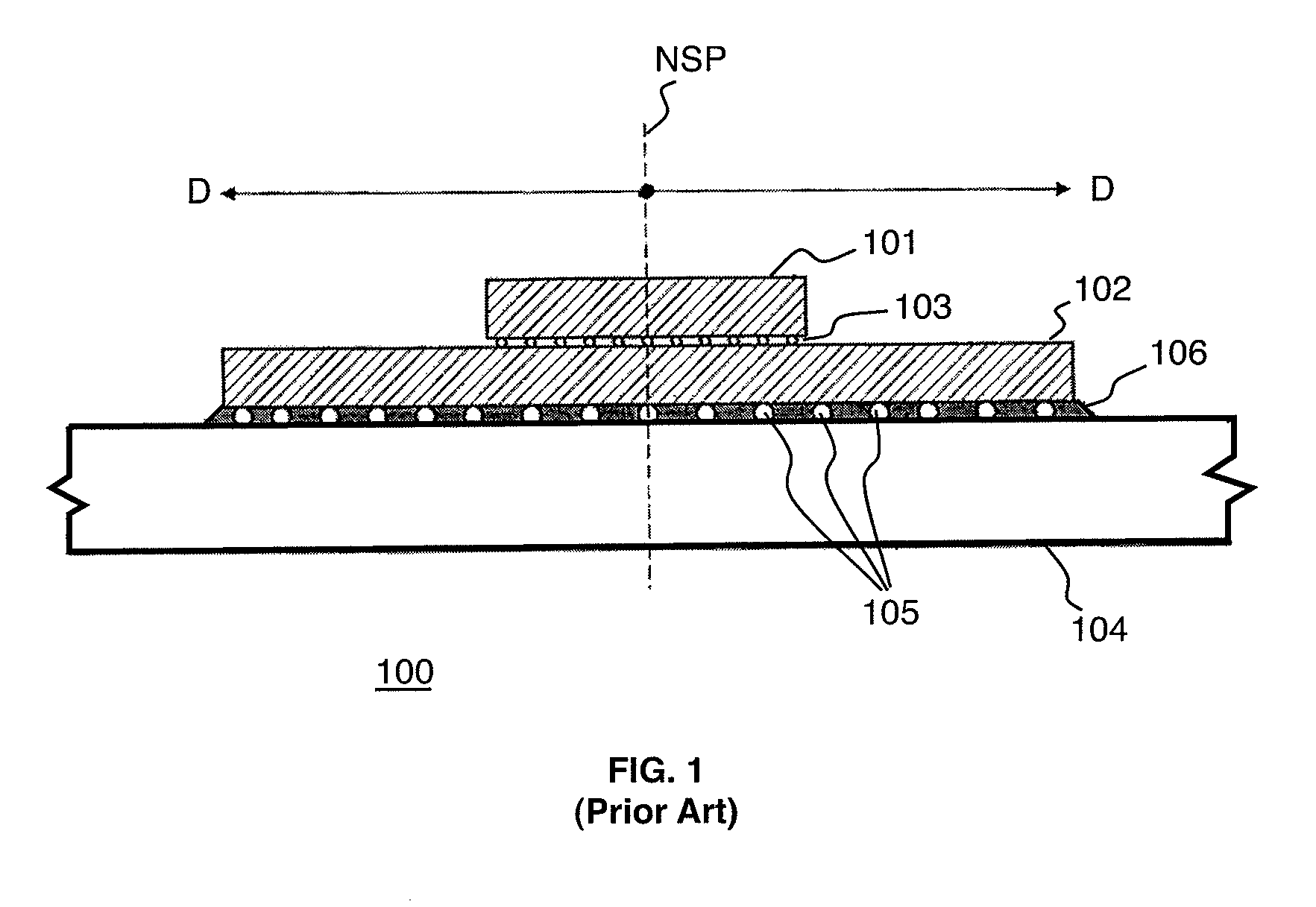
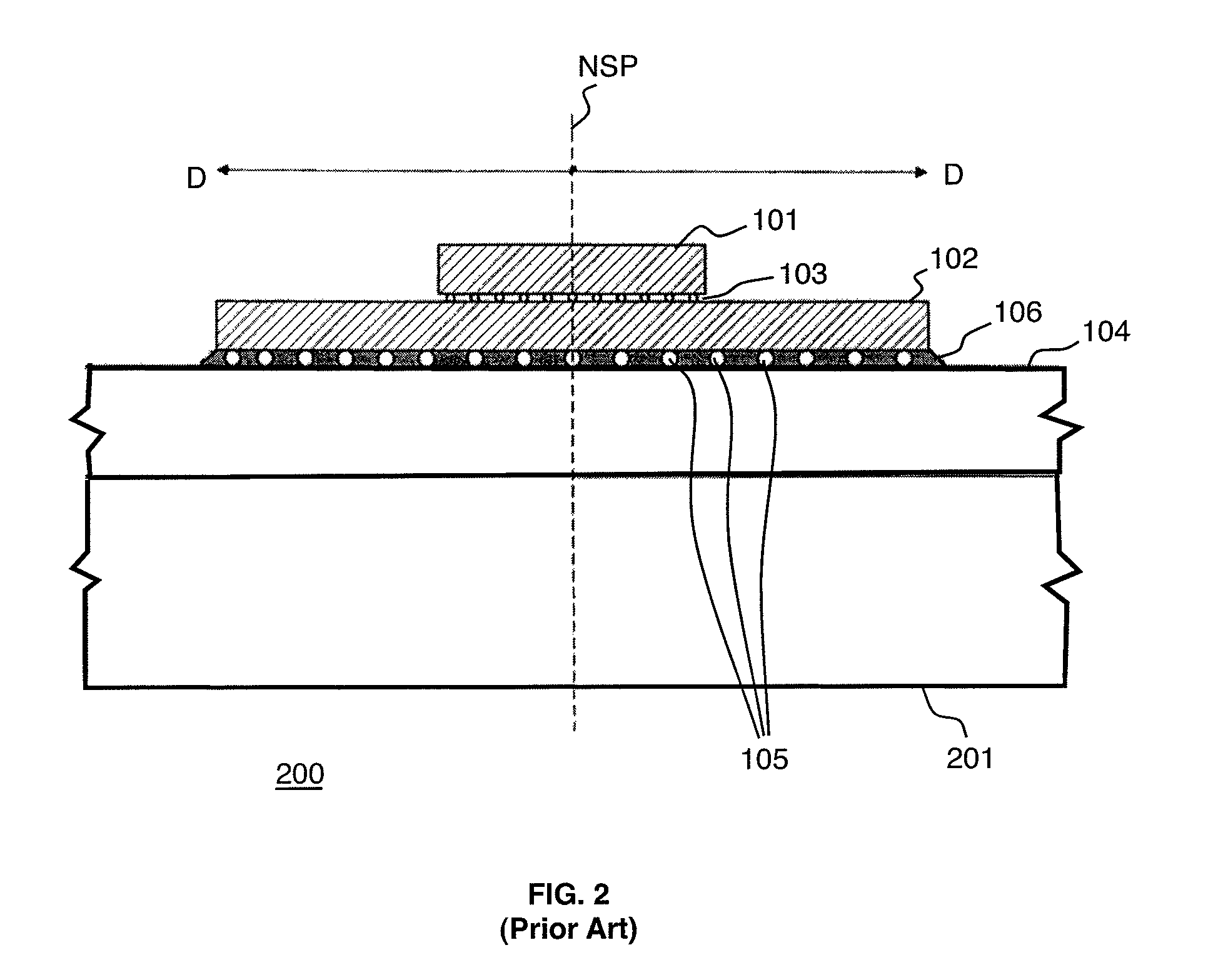
[0021]FIGS. 3A-3B are schematic side-view illustrations of a package structure according to exemplary embodiments of the invention. In general, FIGS. 3A-3B illustrate a package structure (300) comprising a semiconductor IC chip (101), a carrier substrate (102), C4 connections (103), an organic substrate (104), C4 connections (105), and underfill material (106), similar to that discussed above with reference to FIG. 1. In the following discussion, the structure comprising chip (101), connections (103) and chip carrier substrate (102) is referred to as a system-on-package structure (SOP) (110).

[0022]In addition, the exemplary package structure (300) comprises a first stiffener plate (301) bonded to a surface of the organic substrate (104). In contrast to the package structure of FIG. 2, the first stiffener plate (301) comprises a cutout region (301a) (or aperture region). Moreover, the package structure (300) comprises a second stiffener plate (302) that is bonded to the organic subst...


PUM


Abstract

Apparatus and methods are provided for constructing balanced semiconductor chip package structures that minimize bowing, in-plane strain and / or other thermally induced mechanical strains that may arise during thermal cycling, to thus prevent structural damage to chip package structures.

Description

FEDERALLY SPONSORED RESEARCH AND DEVELOPMENT[0001]This invention was made with Government support under Contract No. MDA972-03-3-0004 awarded by Defense Advanced Research Projects Agency. The Government has certain rights in this invention.TECHNICAL FIELD OF THE INVENTION[0002]The present invention relates generally to microelectronic packaging of semiconductor chips and, more specifically, apparatus and methods for constructing balanced semiconductor chip package structures that minimize or prevent bowing, in-plain expansion and / or other thermally induced mechanical strains that can cause structural damage to chip package structures.BACKGROUND[0003]Advances in semiconductor chip fabrication and packaging technologies has enabled development of highly integrated semiconductor chip devices and compact chip package structures (or electronic modules). As chip geometries are scaled down and operating speeds are increased and chip packages become more compact, however, power densities ar...

Claims


Application Information

Patent Timeline
Patent Type & Authority Patents(United States)
IPC IPC(8): H01L23/02H01L29/40
CPCH05K1/0271H01L23/562H01L2224/16H01L2224/83102H01L2224/92125H01L2924/15311H05K1/181H05K3/0058H05K2201/068H05K2201/10734H05K2201/10977H05K2201/2009H01L2924/10253H01L2924/00H01L2924/00014H01L2924/00011H01L2224/0401
Inventor GAYNES, MICHAEL ANTHONYHINGE, KATHLEEN CONLONKNICKERBOCKER, JOHN ULRICH
Owner GLOBALFOUNDRIES INC
Why Eureka
Try Eureka