Fin shaped structure and method of forming the same

a technology of fets and fins, applied in the direction of transistors, electrical devices, semiconductor devices, etc., can solve the problems of increasing the cost of fets, so as to improve vth sensitivity and electric properties, avoid fet structure damage, and preferable vth sensitivity

Active Publication Date: 2016-05-19
UNITED MICROELECTRONICS CORP
View PDF5 Cites 13 Cited by
  • Summary
  • Abstract
  • Description
  • Claims
  • Application Information

AI Technical Summary

Benefits of technology

[0010]Through the present invention, a fin shaped structure having preferable Vth sensitivity may be provided via forming a threshold voltage region after performing the etching back process of the insula

Problems solved by technology

However, as the size of the field effect transistors (FETs) is continuously shrunk, the development of the planar FETs faces more limitations in the fabricating process thereof.
However, since the properties requirements for the shrunken FinFETs become more demanding, the cu

Method used


Image

  • Fin shaped structure and method of forming the same
  • Fin shaped structure and method of forming the same
  • Fin shaped structure and method of forming the same

Examples


Embodiment Construction

[0014]In the following description, numerous specific details, as well as accompanying drawings, are given to provide a thorough understanding of the invention. It will, however, be apparent to one skilled in the art that the invention may be practiced without these specific details.

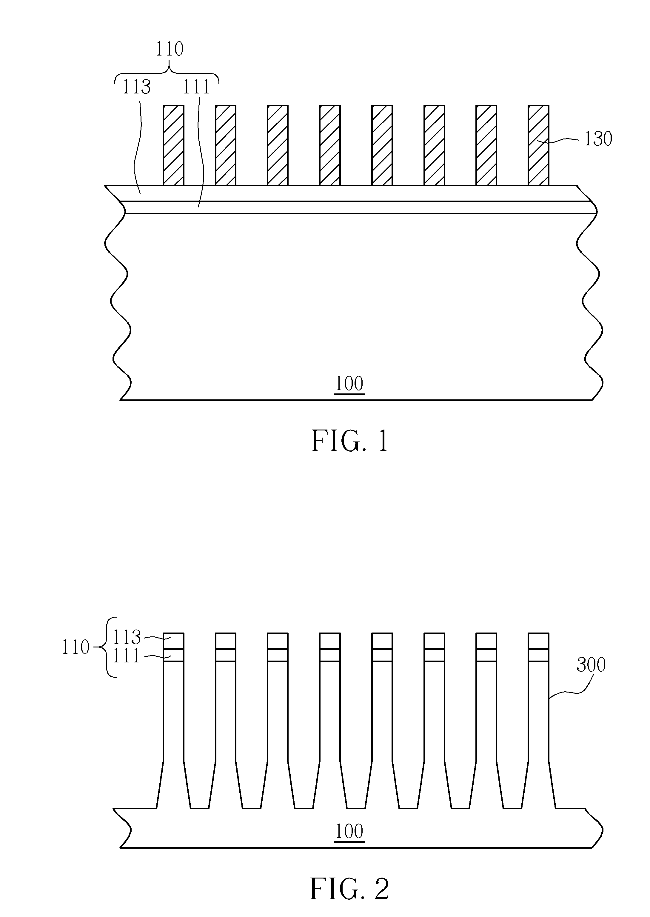
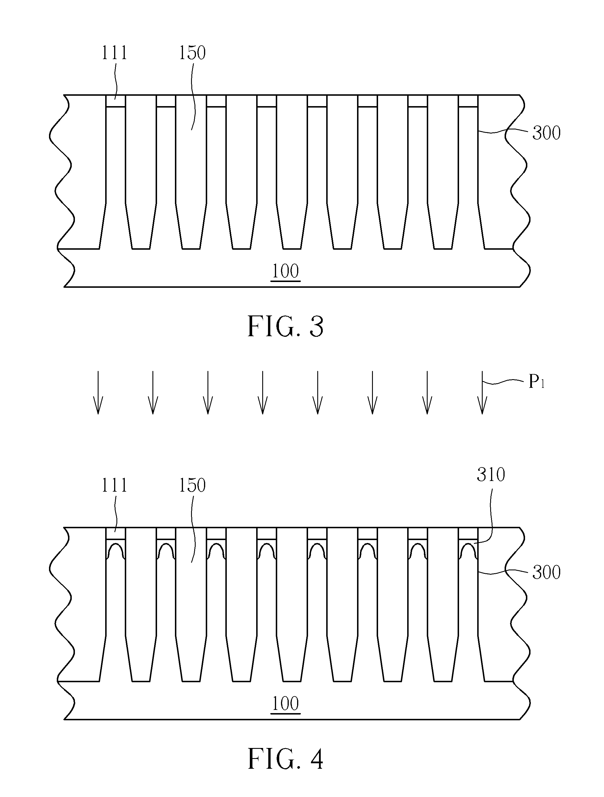
[0015]Referring to FIGS. 1-5, FIGS. 1-5 are schematic diagrams illustrating a method of forming a fin shaped structure according to a first preferred embodiment of the present invention. First of all, as shown in FIGS. 1-2, a substrate 100 is provided, and a hard mask layer 110 is formed on the substrate 100. Precisely speaking, the substrate 100 for example is a semiconductor substrate, including silicon substrate, silicon germanium substrate, silicon carbide substrate, or silicon on insulator (SOI). The hard mask layer 110 is entirely formed on a top surface of the substrate 100, for example, through a chemical vapor deposition (CVD) process or a physical vapor deposition (PVD) process. The hard mask l...


PUM


Abstract

A fin shaped structure and a method of forming the same, wherein the method includes forming a fin structure on a substrate. Next, an insulation layer is formed on the substrate and surrounds the fin structure, wherein the insulation layer covers a bottom portion of the fin structure to expose an exposed portion of the fin structure protruded from the insulation layer. Then, a buffer layer is formed on the fin structure. Following this, a threshold voltage implantation process is performed to penetrate through the buffer layer after forming the insulation layer, to form a first doped region on the exposed portion of the fin structure.

Description

BACKGROUND OF THE INVENTION[0001]1. Field of the Invention[0002]The present invention relates to a fin shaped structure and a method of forming the same, and more particularly to a fin shaped structure having a threshold voltage (Vth) region disposed at the whole exposed surface of the fin shaped structure, and a method of forming the same.[0003]2. Description of the Prior Art[0004]With increasing miniaturization of semiconductor devices, it is crucial to maintain the efficiency of miniaturized semiconductor devices in the industry. However, as the size of the field effect transistors (FETs) is continuously shrunk, the development of the planar FETs faces more limitations in the fabricating process thereof. On the other hand, non-planar FETs, such as fin field effect transistor (FinFET) have three-dimensional structure, not only capable of increasing the contact to the gate but also improving the controlling of the channel region, such that the non-planar FETs have replaced the plan...

Claims


Application Information

Patent Timeline
IPC IPC(8): H01L29/66H01L21/265H01L29/06H01L21/308H01L29/10H01L21/311H01L29/78H01L21/02
CPCH01L29/66537H01L29/7851H01L21/26586H01L21/02236H01L29/0653H01L21/308H01L29/1041H01L29/66795H01L21/311H01L21/02304H01L29/66803H01L29/785
Inventor TSENG, I-MINGHUANG, RAI-MINHUANG, TONG-JYUNLI, KUAN-HSIENHUANG, CHEN-MING
Owner UNITED MICROELECTRONICS CORP
Why Eureka
Try Eureka