Micro-castellated interposer

a micro-castellated and interposer technology, applied in the field of highly packaged products, can solve the problems of high cost, high cost, and high cost of custom parts, and achieve the effect of ensuring reliability and reducing cos

Active Publication Date: 2009-03-24
HONEYWELL INT INC
View PDF10 Cites 18 Cited by
  • Summary
  • Abstract
  • Description
  • Claims
  • Application Information

AI Technical Summary

Benefits of technology

[0019]A primary advantage of the present invention is that it provides a means for circuitry and part changes at the lowest cost with the highest reliability without compromising performance.

Problems solved by technology

As electronic devices get smaller and smaller the prior art methods of part substitution and repair of circuitry create errors on existing hardware and become very problematic, if not entirely troublesome.
Such a custom part is very expensive, requires extensive lead-time and is not compliant to the volume allocated to the existing electronics.
This method is not adequate for an individual revision as it is cost prohibitive.
Scrapping product and re-layout of circuitry is costly and often causes delays in build schedules.
Manual rework is not exact, is prone to human error and adds additional expense due to the use of highly skilled labor.
Additionally, some product still gets scrapped due to damage during repair and the rework is not precise and may introduce variability in electrical integrity.
As parts get smaller, the manual repair and replacement of parts becomes harder and at some point impossible due to human limitations.
A re-layout of the base circuit board can accomplish the same function, that of rewiring, accommodating part changes and providing high reliability, however this approach would be extremely expensive.
Additionally, this method may introduce additional errors in re-layout of complex very high-density circuitry by rerouting of critical signals.
There are several prior art documents that disclose castellations and / or outer land grid pads however, they do not address any context of providing a durable interconnect containing the combination of substrate design / materials, pad geometries, and castellation matched to the parent printed wiring board.
Additionally, the intent of utilizing existing parent printed wiring board circuitry and providing changed electrical functionality that is both manufacturable and low cost is not addressed in any of the prior art.
U.S. Pat. No. 6,377,464 B1 is a device which may have castellations for termination, but does not address durability of the interconnect.
In fact, the method described for constellating a part lacks features, which could provide the necessary durability, namely bottom pads.
While it mentions that the individual “castellations area able to flex (on a microscopic level)” and it allows that the molded material may be matched to the “second component” it does not address how the castellations really flex and if this would be of any benefit to the level of stresses induced due to thermal coefficient of expansion mismatch, not to mention differential heating and cooling.
None of the prior art documents teach or disclose the combination of substrate design / materials, pad and castellation geometries, which allow the formation of a robust solder joint.
Additionally, the prior art fails to disclose the utilization of existing parent printed wiring board circuitry and providing changed electrical functionality that is both manufacturable and low cost.

Method used


Image

  • Micro-castellated interposer
  • Micro-castellated interposer
  • Micro-castellated interposer

Examples


Embodiment Construction

Best Modes For Carrying Out The Invention

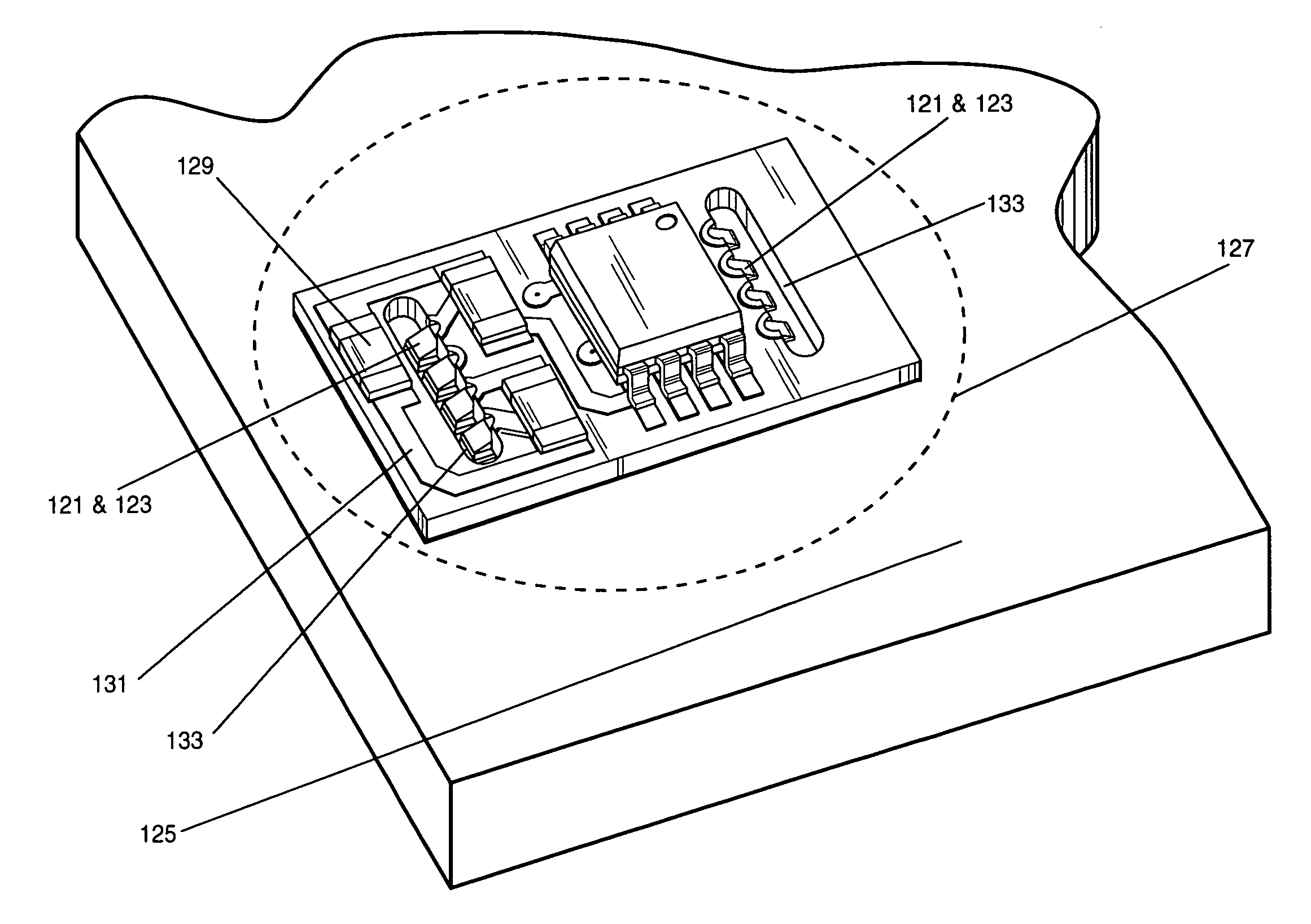
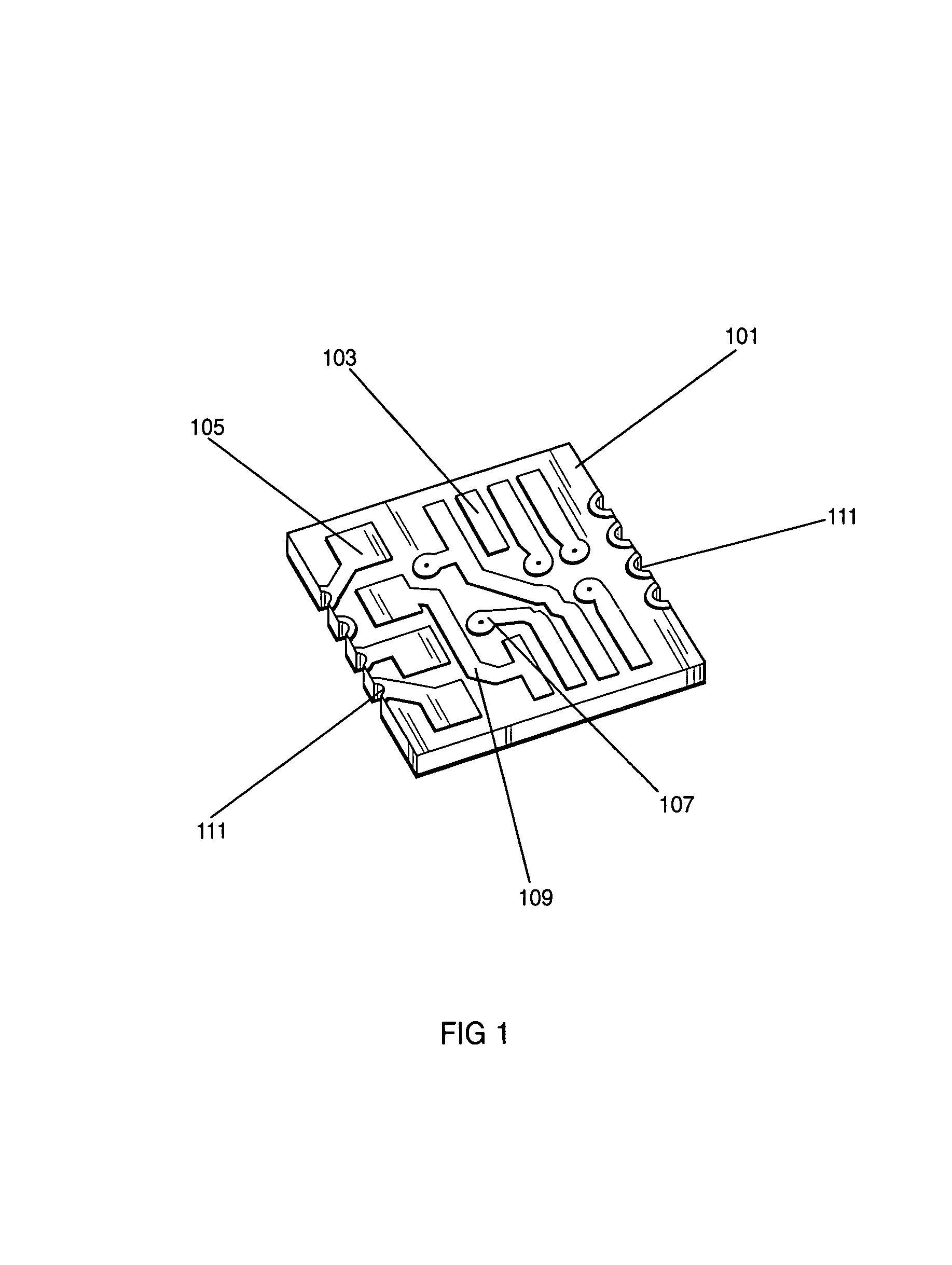
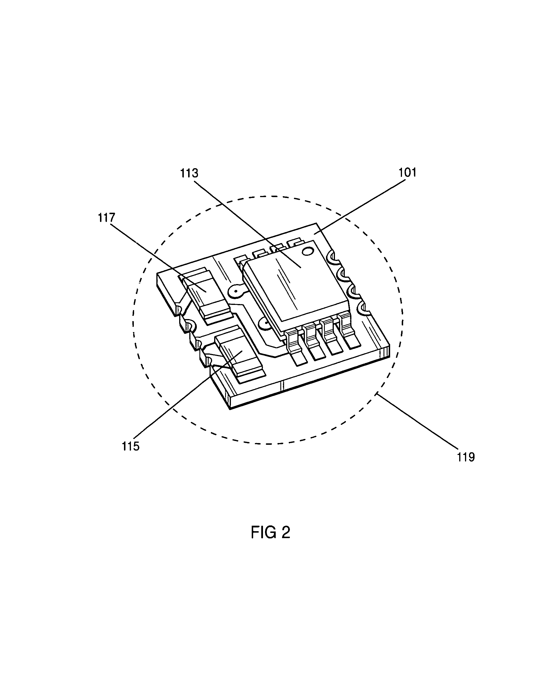
[0027]The present invention comprises a small but common printed circuit board, which can be manufactured with conventional high precision techniques. The layout of this printed circuit board, which can be done in-house to accommodate interface data from the parent circuit card assembly, uses standard trace routing and interconnect (through-holes) found in printed circuit applications. Exact shape, layering and interconnect are determined at the time of laying out the circuitry. Replacement parts and additional parts are incorporated into the circuitry. The micro-castellations which will subsequently interconnect the micro-castellated interconnect board to its parent are placed to optimize circuitry issues while ensuring a robust solder joint which provides the interconnect. Manufacturing methods for the micro-castellated features may vary depending upon the design intent. This design once completed is panelized to provide fabrication efficie...


PUM


Abstract

A miniature PWB with features that incorporate the required circuitry changes and component footprints, which has been enhanced with micro-castellations such as those found on ceramic surface mount packages. The miniature PWB is mounted on the circuit board using techniques well known in the art. This combination of technologies provides an adaptable, durable interconnect methodology, which allows for circuit and part changes without changing the layout of the base printed wiring board.

Description

CROSS-REFERENCE TO RELATED APPLICATIONS[0001]This application is based on U.S. Provisional Application Ser. No. 60 / 584,025 entitled “Micro Castellated Interposer”, filed on Jun. 30, 2004, the teachings of which are incorporated herein by reference.BACKGROUND OF THE INVENTION[0002]1. Field of the Invention (Technical Field):[0003]The present invention relates to packaging of highly reliable, high-speed complex electronics, and more particularly to a method and apparatus for reworking circuits using a micro-castellated interconnect board with its related electrical parts and affixing it to the circuitry.[0004]2. Background Art[0005]As electronic devices get smaller and smaller the prior art methods of part substitution and repair of circuitry create errors on existing hardware and become very problematic, if not entirely troublesome. Repair of circuitry and rewiring of devices on high-speed circuitry needs to be manufacturable and to a great extent electrically identical and meet envi...

Claims


Application Information

Patent Timeline
Patent Type & Authority Patents(United States)
IPC IPC(8): H05K1/16H01L21/48
CPCH01L21/485H01L23/49805H05K1/141H05K3/403H05K3/225H05K3/3442H05K2201/068H05K2201/09063H05K2201/09181H05K2201/09645H01L2924/0002H01L2924/00H01L21/48
Inventor LEVINE, AARONSTANKE, JAY D.
Owner HONEYWELL INT INC
Why Eureka
Try Eureka