Gallium nitride-based compound semiconductor light-emitting device and negative electrode thereof

a compound semiconductor and light-emitting device technology, applied in the direction of semiconductor devices, basic electric elements, electrical appliances, etc., can solve the problems of negative electrode characteristics deteriorating, electrodes cannot be provided on the back surface of the substrate, and high-intensity light is difficult to achieve conventionally, and achieve excellent ohmic contact. , high efficiency

Active Publication Date: 2009-04-14
TOYODA GOSEI CO LTD
View PDF6 Cites 0 Cited by
  • Summary
  • Abstract
  • Description
  • Claims
  • Application Information

AI Technical Summary

Benefits of technology

[0008]An object of the present invention is to provide a negative electrode which attains excellent Ohmic contact with an n-type gallium nitride-based compound semiconductor layer, which resists deterioration, in characteristics, which would be caused by heating, and which can be produced at high efficiency. Another object of the invention is to provide a gallium nitride-based compound semiconductor light-emitting device having the negative electrode.
[0035]The negative electrode according to the present invention has a contact metal layer comprising a Cr—Al alloy. Thus, the negative electrode attains excellent Ohmic contact with an n-type gallium nitride-based compound semiconductor layer and is not deteriorated, in characteristics, by heating. Such an excellent Ohmic contact between the negative electrode of the present invention and the n-type gallium nitride-based compound semiconductor layer can be provided without performing annealing. Therefore, the gallium nitride-based compound semiconductor light-emitting device of the present invention can be produced with remarkably high efficiency.

Problems solved by technology

Through employment of such a compound semiconductor, ultraviolet light, blue light, or green light of high emission intensity can be obtained; such high-intensity light has conventionally been difficult to attain.
Unlike the case of a GaAs light-emitting device, such a gallium nitride-based compound semiconductor is generally grown on a sapphire substrate (i.e., an insulating substrate); hence, an electrode cannot be provided on the back surface of the substrate.
However, when heated, the negative electrode has deteriorated characteristics.
However, as the above method includes a thermal annealing step after formation of a negative electrode, productivity of the electrode is unsatisfactory.

Method used


Image

  • Gallium nitride-based compound semiconductor light-emitting device and negative electrode thereof
  • Gallium nitride-based compound semiconductor light-emitting device and negative electrode thereof

Examples


examples

[0053]The present invention will next be described in more detail by way of Examples and Comparative Examples. Table 1 shows negative electrode materials employed in the Examples and Comparative Examples, and evaluation of characteristics immediately after formation of a negative electrode film and after a heating test. Needless to say, these Examples and Comparative Examples should not be construed as limiting the invention.

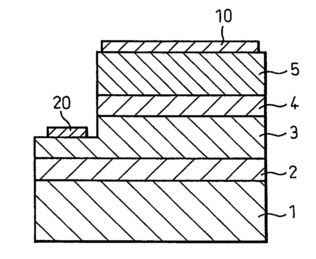
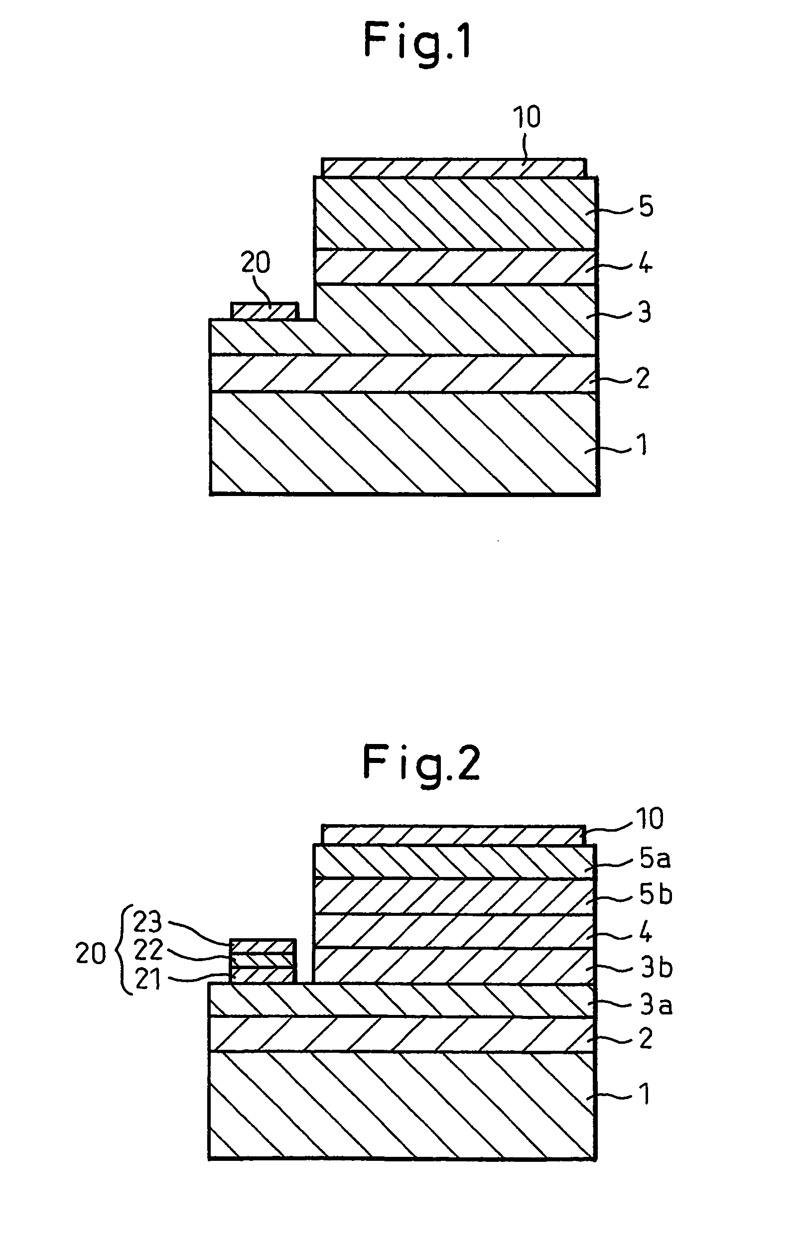
[0054]FIG. 2 is a schematic view showing a gallium nitride-based compound semiconductor light-emitting device produced in the present Example.

[0055]The gallium nitride-based compound semiconductor stacked structure employed for fabricating the light-emitting device was produced through the following procedure: an AlN buffer layer 2 was formed on a sapphire substrate 1; and an n-type GaN contact layer 3a, an n-type GaN lower cladding layer 3b, an InGaN light-emitting layer 4, a p-type AlGaN upper cladding layer 5b, and a p-type GaN contact layer 5a were successiv...


PUM


Abstract

A gallium nitride-based compound semiconductor light-emitting device is disclosed which includes an n-type semiconductor layer of a gallium nitride-based compound semiconductor, a light-emitting layer of a gallium nitride-based compound semiconductor and a p-type semiconductor layer of a gallium nitride-based compound semiconductor formed on a substrate in this order, and has a negative electrode and a positive electrode provided on the n-type semiconductor layer and the p-type semiconductor layer, respectively. The negative electrode includes a bonding pad layer and a contact metal layer which is in contact with the n-type semiconductor layer, and the contact metal layer is composed of a Cr—Al alloy.

Description

CROSS REFERENCE TO RELATED APPLICATION[0001]This application is an application filed under 35 U.S.C. §111(a) claiming benefit, pursuant to 35 U.S.C. §119(e) (1), of the filing date of the Provisional Application No. 60 / 532,722 filed on Dec. 29, 2003, pursuant to 35 U.S.C. §111(b).TECHNICAL FIELD[0002]The present invention relates to a gallium nitride-based compound semiconductor light-emitting device, and more particularly to a flip-chip-type gallium nitride-based compound semiconductor light-emitting device having a negative electrode that exhibits excellent characteristics and can be fabricated with high productivity.BACKGROUND ART[0003]In recent years, gallium nitride-based compound semiconductors represented by the formula AlxGayIn1-x-yN (0≦x≦1, 0≦y≦1, x+y≦1) have become of interest as materials for producing a light-emitting diode (LED) which emits ultraviolet to blue light, or green light. Through employment of such a compound semiconductor, ultraviolet light, blue light, or g...

Claims


Application Information

Patent Timeline
Patent Type & Authority Patents(United States)
IPC IPC(8): H01L27/15H01L21/28H01L21/285H01L33/06H01L33/32H01L33/38H01L33/40H01L33/62
CPCH01L21/28575H01L33/40H01L33/32
Inventor KAMEI, KOJI
Owner TOYODA GOSEI CO LTD
Why Eureka
Try Eureka