Deposition pattern for eliminating backside metal peeling during die separation in semiconductor device fabrication

a technology of die separation and die separation pattern, which is applied in the direction of semiconductor devices, semiconductor/solid-state device details, electrical equipment, etc., can solve the problems of bm layer often damaged (, torn, delaminated, etc., and bm layer to tear across the break lin

Active Publication Date: 2009-04-14
SUMITOMO ELECTRIC DEVICE INNOVATIONS U S A
View PDF3 Cites 3 Cited by
  • Summary
  • Abstract
  • Description
  • Claims
  • Application Information

AI Technical Summary

Benefits of technology

[0014]A method of protecting metal traces and contacts on a fabricated semiconductor wafer from mechanical damage during dicing of the fabricated wafer, where the metal traces and contacts form electrical connections with an active device region of the semiconductor. The method includes the steps of providing a group of discrete metal deposits adjacent the metal traces and contacts, wherein said metal deposits are substantially not contiguously connected to each other or to any traces or contacts of the active device regions of semiconductor die, attaching the fabricated wafer to an adhesive tape used for securing the fabricated wafer during a die separation process, separating the die from the fabricated wafer while attached to the adhesive tape and removing the die from the adhesive tape.

Problems solved by technology

Because semiconductors tend to be hard and brittle, while the metal (e.g., Au / Ge—NI—Au) of the connections is soft and ductile, the BM layer is often damaged (e.g., torn, delaminated, etc.) when the die are separated.
Scribing and breaking wafers often causes the BM layer to tear across a break line.
Sawing often causes small chips to be dislodged adjacent the saw kerf, thereby loosening the edges of the BM layer adjacent the saw kerf.
The metal burrs on the bottom of the die cause misalignment during use by causing the die to rest at an angle when placed on a flat surface.
When placed into a final package the misalignment of the top surface of the die can degrade the performance of devices optically connected with the die.
In addition, the tilted die degrades the quality of wire bonds and reduces the ability of the package to extract heat from active devices.
Both conditions can cause long-term quality and reliability concerns.
Because the tearing process is inherently random, tearing contributes to process variability in integrated circuit production and use.
In addition, the trend towards smaller die increases the variability caused by torn and / or delaminated metal.
For a given area of torn metal, the smaller die will also result in a greater percentage of total area being damaged.
The increased tackiness increases the incidence of damage.

Method used


Image

  • Deposition pattern for eliminating backside metal peeling during die separation in semiconductor device fabrication
  • Deposition pattern for eliminating backside metal peeling during die separation in semiconductor device fabrication
  • Deposition pattern for eliminating backside metal peeling during die separation in semiconductor device fabrication

Examples


Embodiment Construction

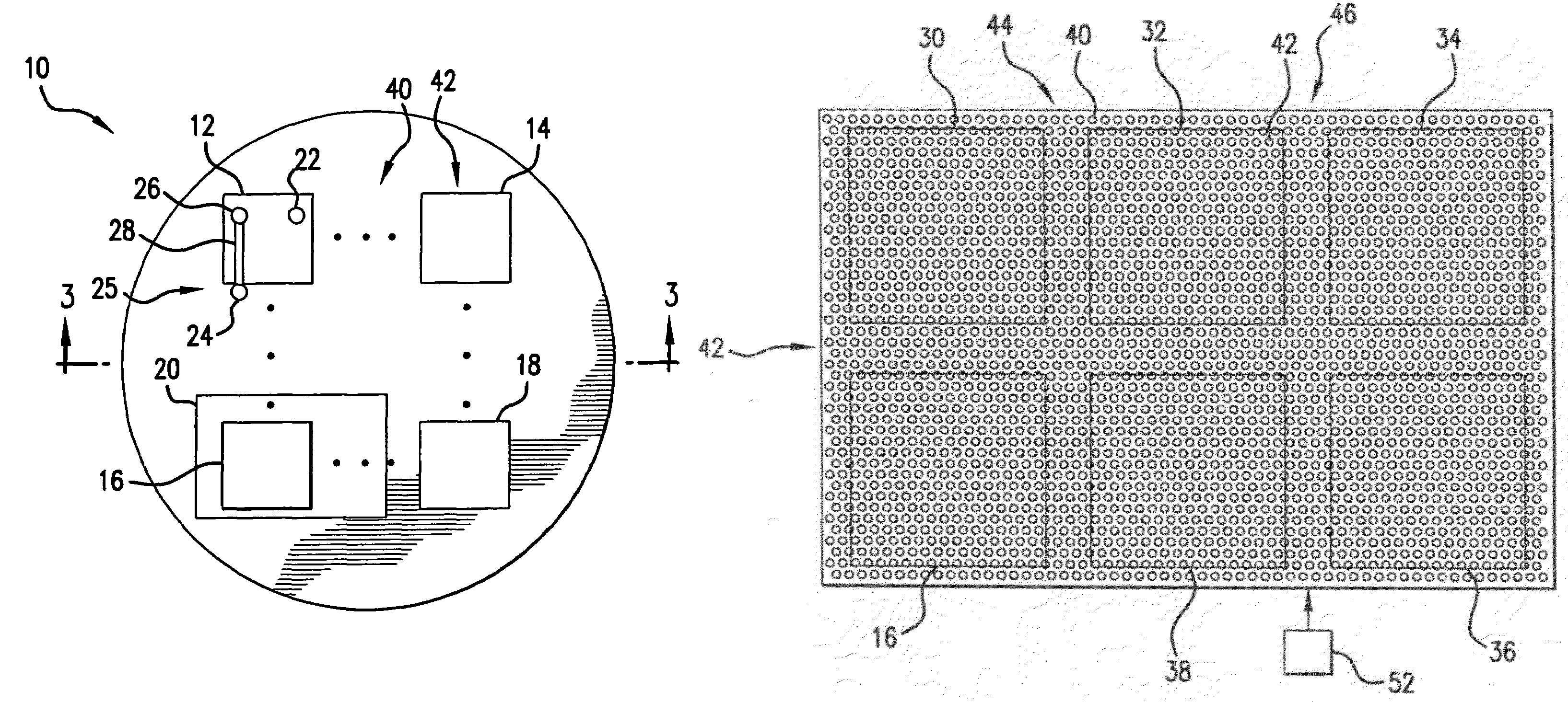
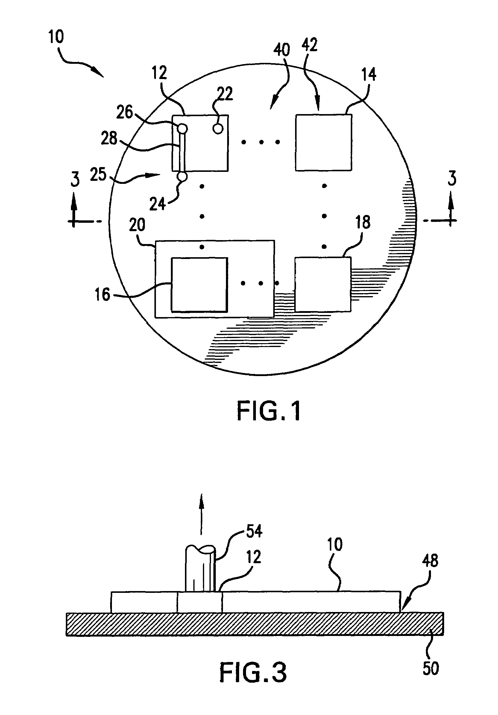
[0020]FIG. 1 is a bottom view of a fabricated wafer 10 under illustrated embodiments of the invention. A fabricated wafer is a wafer upon which a number of integrated circuits have been constructed by conventional techniques (except as noted below) and which wafer needs to be separated into one or more die in order to serve its intended function.

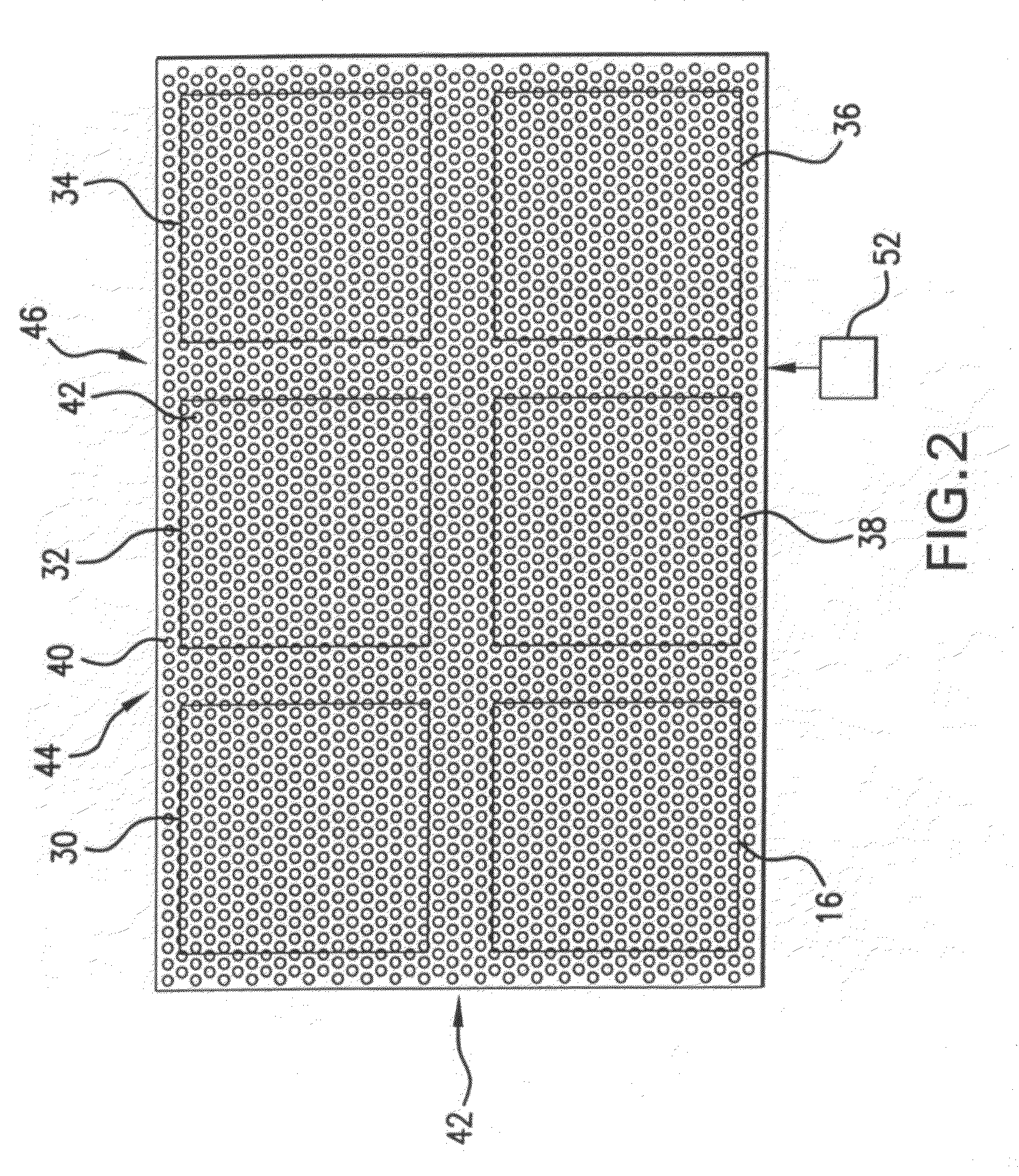
[0021]Under illustrated embodiments, the wafer 10 may be fabricated with a group of metal deposits (dots) 40, 42 on a backside of the wafer 10. The backside of the wafer is the side of the wafer that would be attached to the adhesive of a saw frame during a separation process.

[0022]The group of metal dots may be disposed adjacent to and around any metal structure disposed on the backside of the wafer 10. The presence of the metal dots has been found to retard the occurrence of burrs on backside metal structures especially adjacent a saw kerf. FIG. 5 is a flow chart that depicts process steps that may be used in conjunction with the metal dot...


PUM


Abstract

A semiconductor wafer that includes a plurality of groups of active devices or circuits on a first side of the wafer and a patterned electrical contact on the backside of the wafer. Each group consisting of an active device or circuit is intended to be diced into a discrete chip. The backside of the wafer includes a metal layer patterned into discrete spaced-apart deposits that form an electrical contact to the semiconductor and the respective group of active devices. The deposits are not contiguously or laterally connected to each other and function to protect the metal layer from peeling or detaching from the wafer during dicing of the semiconductor wafer into chips.

Description

REFERENCE TO RELATED APPLICATIONS[0001]This application is a Divisional of U.S. application Ser. No. 11 / 280,783 filed Nov. 16, 2005 (now U.S. Pat. No. 7,198,988).FIELD OF THE INVENTION[0002]The field of the invention relates to the fabrication of semiconductor wafers and more particularly to quality and reliability associated with the dicing of fabricated semiconductor wafers.BACKGROUND OF THE INVENTION[0003]Integrated circuits are typically fabricated on a wafer of silicon or other appropriate semiconductor. After fabrication of a wafer, the individual chips are separated from the wafer and packaged and interconnected with other circuits in their final application, such as for computers, consumer electronics, etc.[0004]In order to function as intended, the chips of integrated circuits are provided with external electrical connections for use with other circuits. In some designs, certain of the external connections are typically formed by plating metal pads on the bottom (backside) ...

Claims


Application Information

Patent Timeline
Patent Type & Authority Patents(United States)
IPC IPC(8): H01L23/48
CPCH01L21/6836H01L21/78H01L23/562H01L2221/68327H01L2924/0002H01L2924/00
Inventor COLLINS, DOUGLASLIU, LINLINTAYLOR, ELAINE
Owner SUMITOMO ELECTRIC DEVICE INNOVATIONS U S A
Why Eureka
Try Eureka