

Liquid crystal display apparatus
a technology of liquid crystal display and display set, which is applied in the direction of identification means, digital storage, instruments, etc., can solve the problem of enlarging the width of the display s
- Summary
- Abstract
- Description
- Claims
- Application Information
AI Technical Summary
Benefits of technology
Problems solved by technology
Method used
Image

Examples
Embodiment Construction
[0031]Hereinafter, the preferred embodiments of the present invention will be described in detail with reference to the accompanying drawings.
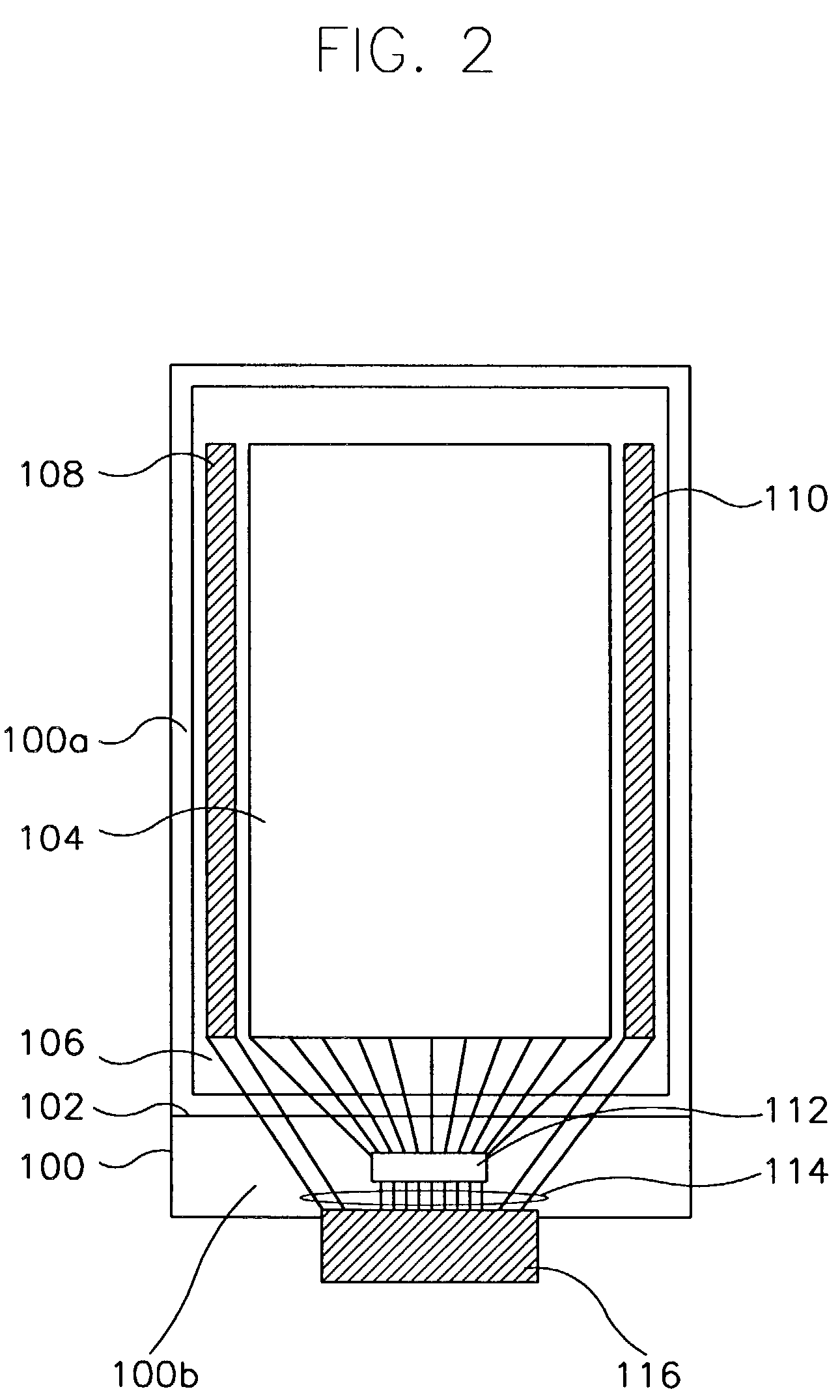
[0032]FIG. 2 is a schematic view showing a symmetric-type liquid crystal display (LCD) module having dual gate driving circuits according to a preferred embodiment of the present invention.
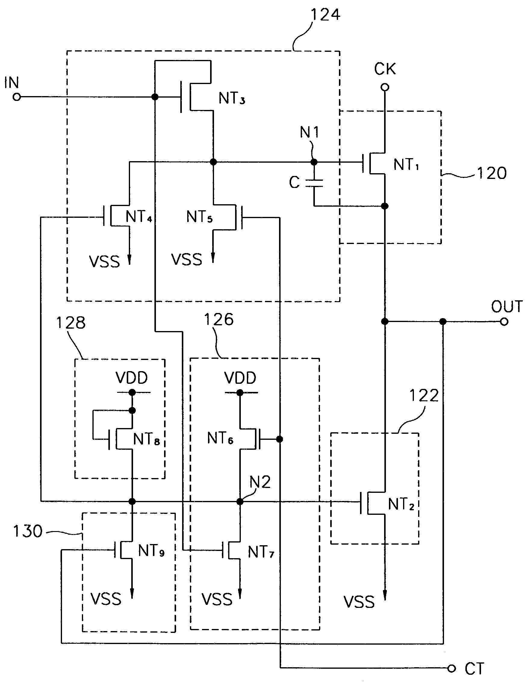
[0033]Referring to FIG. 2, the LCD module includes a lower substrate 100 and an upper substrate 102. The lower substrate 100 is divided into a first region 100a overlapping with upper substrate 102 and a second region 100b without overlapping therewith.
[0034]The first region 100a includes a display region 104 and a peripheral region 106. After a liquid crystal is injected between the lower substrate 100 and the upper substrate 102, a marginal edge portion of the display region 104 and the peripheral region 106 are sealed with a sealing material. A first and a second gate driving circuits 108 and 110 are arranged onto the left and right portions of the periph...
PUM
| Property | Measurement | Unit |
|---|---|---|
| time | aaaaa | aaaaa |
| power | aaaaa | aaaaa |
| voltage | aaaaa | aaaaa |
Abstract
Description
Claims
Application Information