Scanning-line selecting circuit and display device using the same

a selection circuit and display device technology, applied in the direction of static storage, digital storage, instruments, etc., can solve the problems of “threshold value shift” and not exist the same problem, and achieve the effect of stable operation and high efficiency

Active Publication Date: 2009-04-21
PANASONIC LIQUID CRYSTAL DISPLAY CO LTD +1
View PDF10 Cites 9 Cited by
  • Summary
  • Abstract
  • Description
  • Claims
  • Application Information

AI Technical Summary

Benefits of technology

[0008]Also, this means that a variation in the output voltage can be suppressed within a small range when the threshold-value voltage of the switching element varies depending on such factors as a time-lapse factor and a temperature condition.
[0009]It is an object of the present invention to provide a scanning-line selecting circuit and a display device using the same, which are excellent in economy and stability, and which allow the output to be stably maintained independently of such factors as a time-lapse factor and a temperature condition even if input voltage of the scanning-line selecting circuit and voltage amplitude of a scanning-line driving signal are made equal with each other.
[0022]The scanning-line selecting circuit according to the present invention and the display device using the same result in none of the problems of the threshold-value shift and voltage lowering. This characteristic makes it possible to implement high efficiency and stable operation.

Problems solved by technology

Also, in an a-Si (i.e., amorphous-silicon) TFT, there exists a problem of “threshold-value shift” which is characteristic of the a-Si TFT.
Also, it has been found that basically the same problem exists not only in the a-Si TFT also but also in an organic TFT.

Method used


Image

  • Scanning-line selecting circuit and display device using the same
  • Scanning-line selecting circuit and display device using the same
  • Scanning-line selecting circuit and display device using the same

Examples


embodiment 1

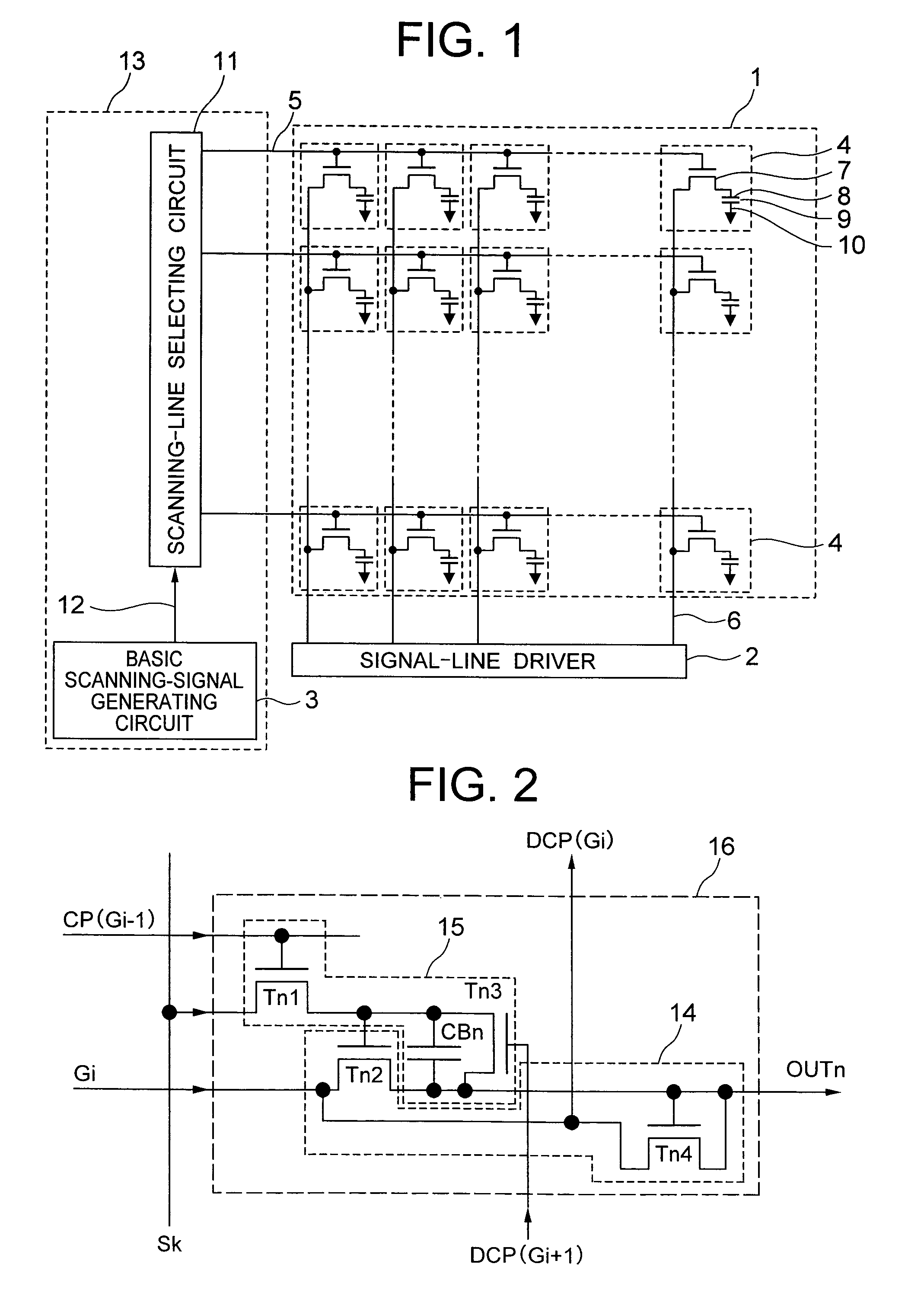
[0045]FIG. 1 is a schematic diagram for illustrating the entire configuration of a display device according to the present invention. This display device includes a display unit 1, a signal-line driver 2, and a scanning-line driving circuit 13. Pixel components 4 are located in a matrix-like configuration on the display unit 1 formed on a glass substrate.

[0046]Each pixel portion 4 has a structure that a thin film transistor (hereinafter, referred to as “TFT”) 7 exists at an intersection point of a signal line 6 and a scanning line 5. A gate terminal of the TFT 7, a first terminal thereof, and a second terminal thereof are connected to the scanning line 5, the signal line 6, and a pixel electrode 8, respectively. Incidentally, although the first terminal and second terminal of the TFT 7 will be explained in a manner of being distinguished from each other, there exists no difference on the function between them.

[0047]A liquid-crystal layer 9 is sandwiched between the pixel electrode 8...

embodiment 2

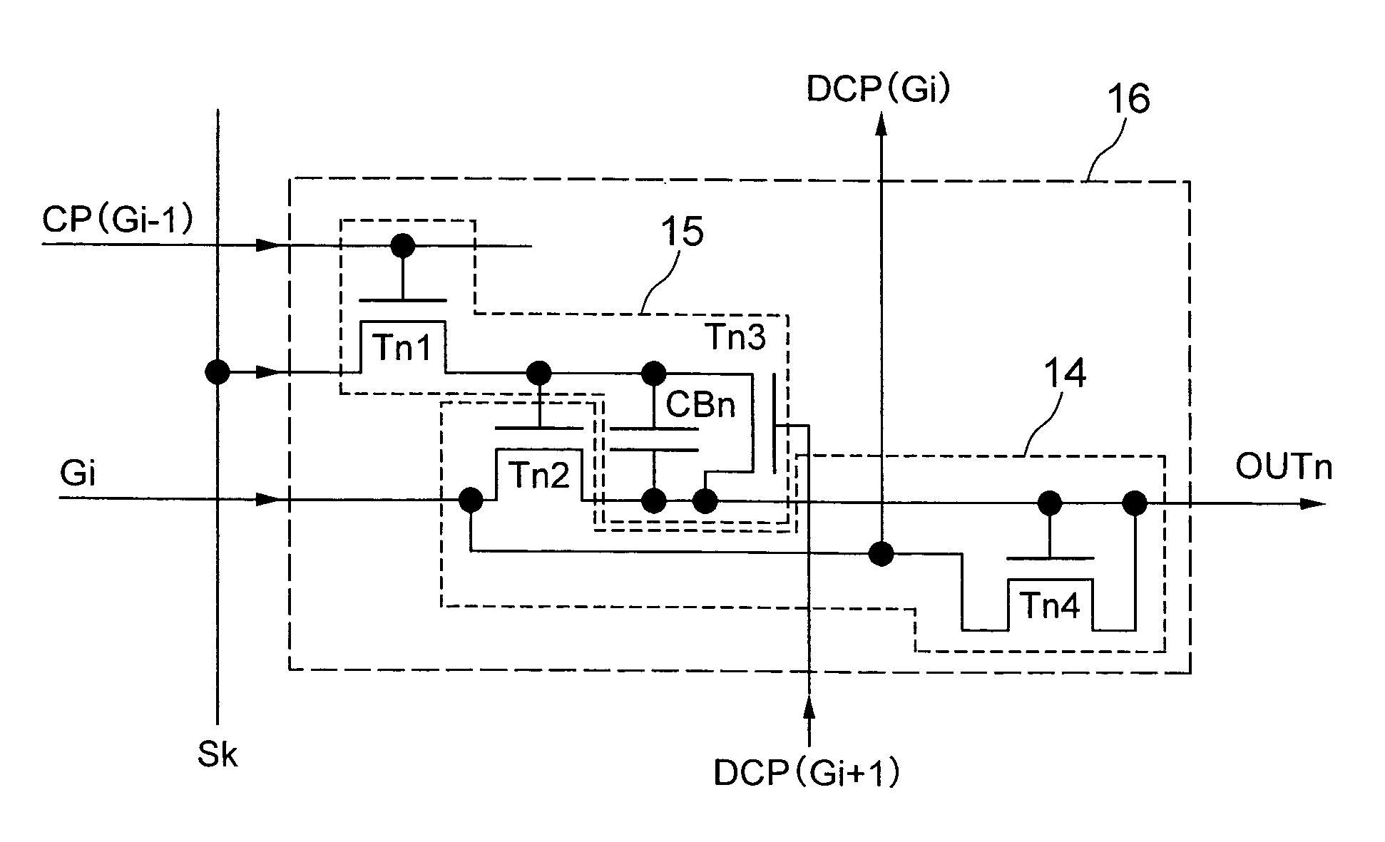
[0052]FIG. 2 is a circuit diagram for illustrating a basic circuit 16 corresponding to an n-th scanning line in the scanning-line selecting circuit 11 illustrated in FIG. 1. This basic circuit 16, which exists in a one-to-one correspondence relationship with one scanning line, includes a basic scanning-line driving circuit 14 and a voltage raising circuit 15.

[0053]The basic scanning-line driving circuit 14 includes a scanning-line driving element Tn2 and a scanning-line stabilizing element Tn4. Also, the voltage raising circuit 15 includes a charge element Tn1, a voltage-raising capacitor CBn, and a discharge element Tn3. These respective elements are MOS transistors formed simultaneously with the TFTs on the display unit 1 and having a structure similar thereto.

[0054]A first terminal of the charge element Tn1 or a selecting-signal input terminal is connected to a corresponding selecting-signal line Sk. A gate terminal thereof or a charge-pulse input terminal is connected to a charg...

embodiment 3

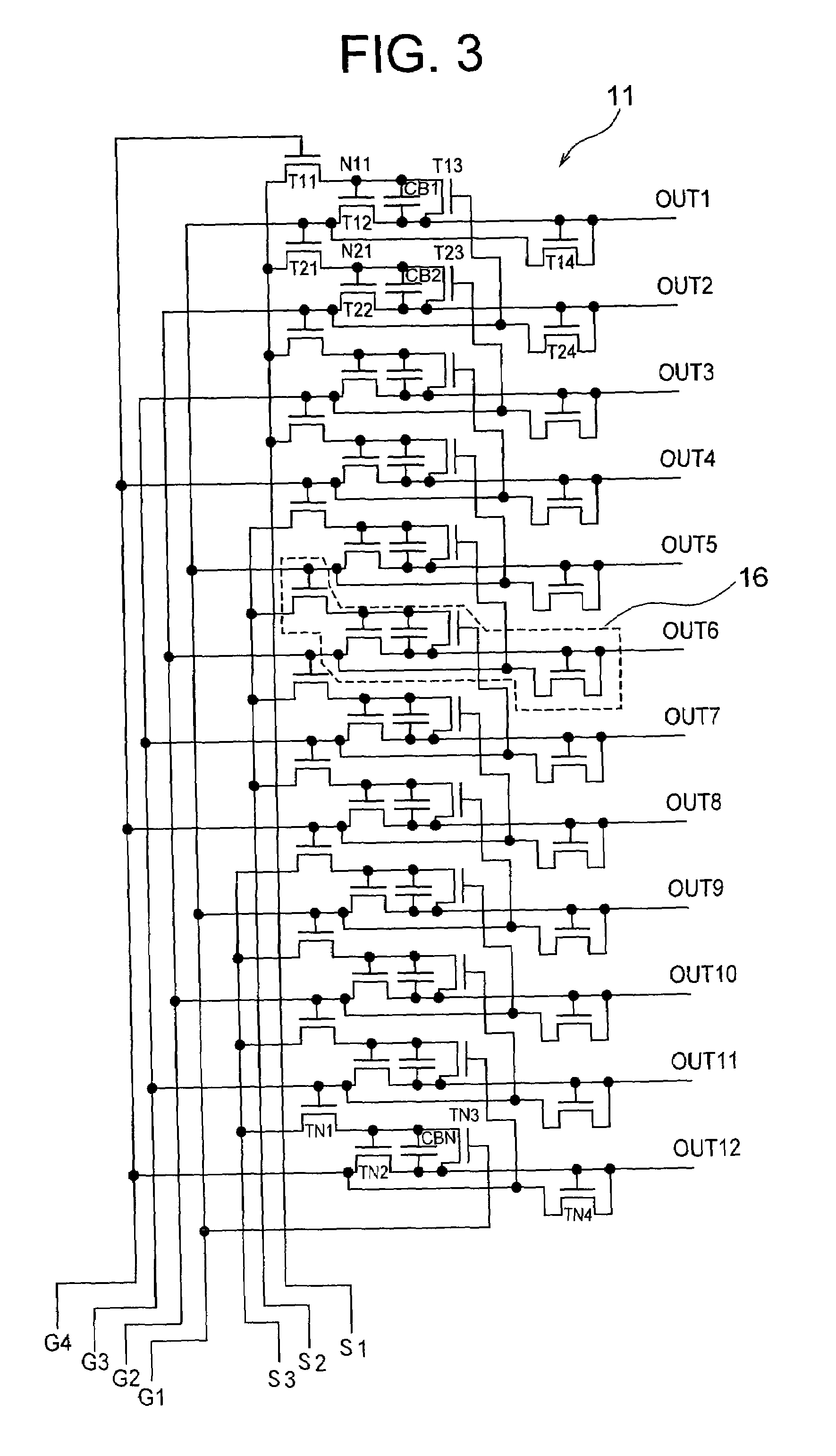
[0080]FIG. 5 is a circuit diagram for illustrating another embodiment of the scanning-line selecting circuit 11 illustrated in FIG. 1. In FIG. 5, a gate terminal of a MOS transistor T11 existing at the first stage and a gate terminal of a MOS transistor TN3 existing at the final stage are connected to an auxiliary-signal line FLMS and an auxiliary-signal line FLME, respectively.

[0081]Also, FIG. 6 illustrates a timing chart for the scanning-line selecting circuit 11 illustrated in FIG. 5. This chart illustrates waveform of a node N11 and that of an output OUT1 with respect to selecting signals S1 to S3, basic scanning signals G1 to G4, and the auxiliary signals FLMS and FLME.

[0082]As illustrated in FIG. 5, at first, a first terminal of the MOS transistor T11 is connected to the selecting signal S1. A gate terminal thereof is connected to the auxiliary signal FLMS. A second terminal thereof or the node N11 is connected to a gate terminal of a MOS transistor T12, a first terminal of a ...


PUM

PropertyMeasurementUnit
voltageaaaaaaaaaa
thresholdaaaaaaaaaa
threshold-aaaaaaaaaa

Abstract

A scanning-line selecting circuit is configured by connecting basic circuits with each other over plural stages. Each of the basic circuits includes a basic scanning-line driving circuit and a voltage raising circuit. A basic scanning signal is inputted into the basic scanning-line driving circuit, which, then, outputs a scanning signal. A charge pulse, a selecting signal, and a discharge pulse are inputted into the voltage raising circuit, which, then, drives the basic scanning-line driving circuit. Accordingly, in the basic circuits, there exists none of the problems of threshold-value shift and voltage lowering. This characteristic makes it possible to implement high efficiency and stable operation.

Description

BACKGROUND OF THE INVENTION[0001]1. Field of the Invention[0002]The present invention relates to a scanning-line selecting circuit and a display device using the same. In particular, it relates to a liquid crystal display, or a TFT (Thin Film Transistor) active-matrix liquid crystal display.[0003]2. Description of the Related Art[0004]From conventionally, a proposal has been made concerning a method for driving all of scanning lines by reducing output number of scanning-line driving IC down to one-several tenths, and also by using a scanning-line selecting circuit. Here, this proposal has been made in order to allow a decrease in implementation cost and driving IC cost, an enhancement in reliability, and a reduction in area of non-display portion.[0005]Also, in an a-Si (i.e., amorphous-silicon) TFT, there exists a problem of “threshold-value shift” which is characteristic of the a-Si TFT. Namely, if a voltage higher or lower than a first terminal (drain or source) and a second termi...

Claims


Application Information

Patent Timeline
Patent Type & Authority Patents(United States)
IPC IPC(8): G09G3/36G02F1/133G09G3/20G11C19/28
CPCG09G3/3677G11C19/28G09G2310/0278G09G3/20G09G3/36
Inventor EDO, SUSUMUKOMURA, SHINICHIHIROTA, SHOICHIISHIGE, NOBUYUKI
Owner PANASONIC LIQUID CRYSTAL DISPLAY CO LTD
Why Eureka
Try Eureka