Variable resistance element, semiconductor device having variable resistance element, semiconductor device manufacturing method, and programming method using variable resistance element

a technology of variable resistance and programming method, which is applied in the field of variable resistance element, semiconductor device manufacturing method, and programming method using variable resistance element, can solve problems such as substantial cost increase, and achieve the effects of reducing programming voltage, reducing programming voltage, and suppressing programming voltage variation

Active Publication Date: 2015-04-16
NANOBRIDGE SEMICON INC
View PDF13 Cites 13 Cited by
  • Summary
  • Abstract
  • Description
  • Claims
  • Application Information

AI Technical Summary

Benefits of technology

[0016]According to the present invention, the shortest distance between both the corners of the first electrode and the second electrode is defined, and therefore a location where a filament (conductive path) is formed is defined. From this, a programming operation can be stabilized, and the variation of a programming voltage can be suppressed to a low level enabling the programming voltage to be lowered.
[0017]Further, since each electrode is a corner, the effective electric field during programming can be intensified due to an effect of electric field concentration, and therefore a programming voltage can be lowered.

Problems solved by technology

However, the gate length of a MOSFET (Metal Oxide Semiconductor Field Effect Transistor) has recently reached 20 nm or less bringing substantial cost increase of a lithography process (device price, and mask set price), and a physical limit of a device dimension (operating limit, or variation limit), and improvement of the device performance by an approach different from the past one depending on the scaling law has come to be sought-after.

Method used


Image

  • Variable resistance element, semiconductor device having variable resistance element, semiconductor device manufacturing method, and programming method using variable resistance element
  • Variable resistance element, semiconductor device having variable resistance element, semiconductor device manufacturing method, and programming method using variable resistance element
  • Variable resistance element, semiconductor device having variable resistance element, semiconductor device manufacturing method, and programming method using variable resistance element

Examples


first embodiment

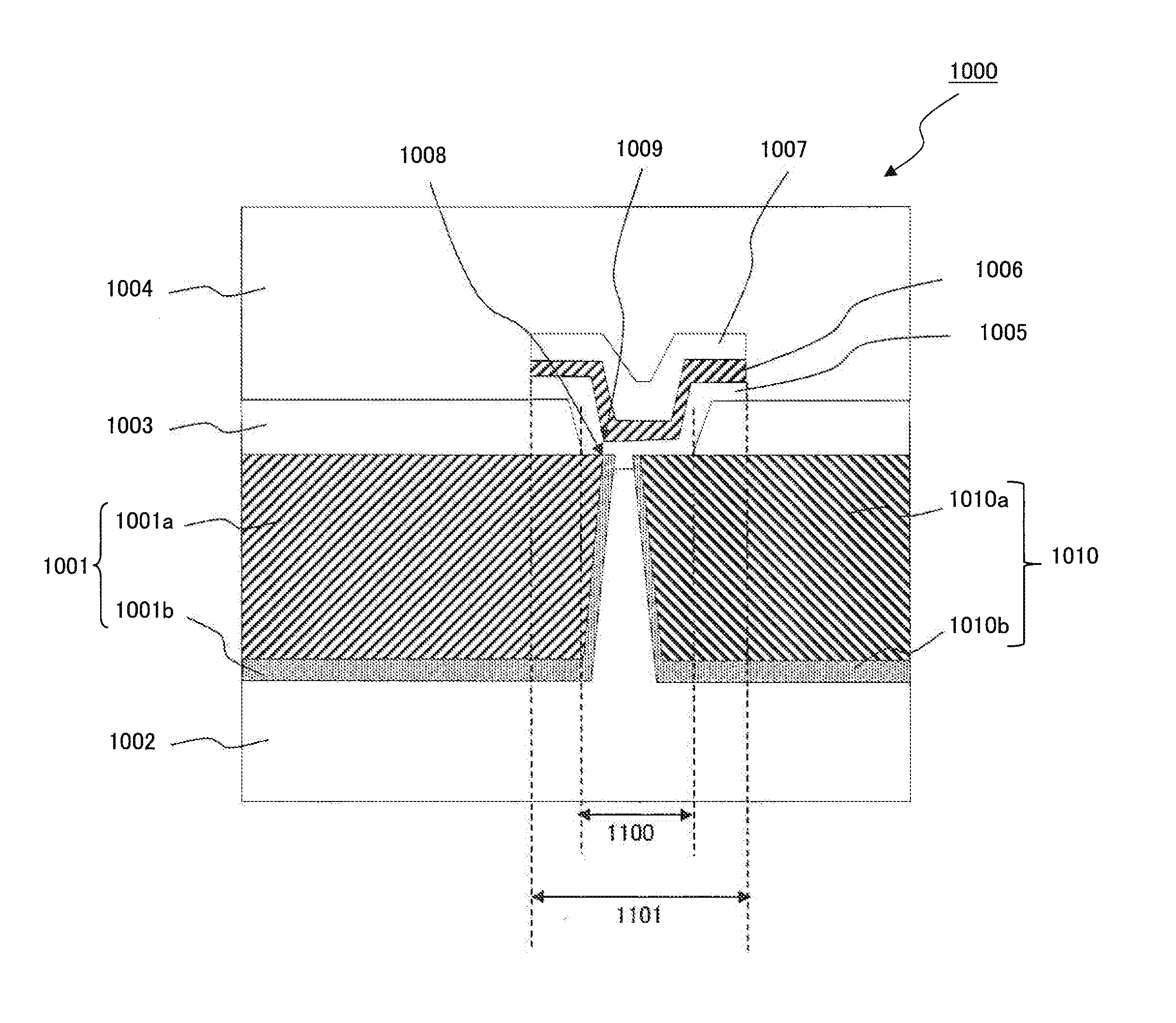
[0050]The constitution of a variable resistance element 100 used in a semiconductor device according to the first Embodiment of the present invention will be described. FIG. 3 is a diagram depicting an exemplar constitution of a variable resistance element to be used in the semiconductor device according to the Embodiment.

[Description of Structure]

[0051]The variable resistance element 100 depicted in FIG. 3 is for example a solid electrolyte switch (atomic switch) presenting bipolar type resistance change operation. It is configured including a first electrode 101 (active electrode), a second electrode 102 (inactive electrode), and a variable resistance film 103 sandwiched by the electrodes. They are formed inside an insulation film 105 on a semiconductor substrate (not illustrated). The variable resistance film 103 is for example an ion conductor disclosed in Non Patent Literature 1.

[0052]The first electrode 101 has a corner of first electrode 106, and the second electrode 102 has ...

second embodiment

[0061]The constitution of a variable resistance element 200 used in a semiconductor device according to the second Embodiment of the present invention will be described. FIG. 4 is a diagram depicting an exemplar constitution of a variable resistance element to be used in the semiconductor device according to the Embodiment.

[Description of Structure]

[0062]As depicted in FIG. 4, the constitution of the second Embodiment is identical with Embodiment 1 except that the positions of the upper surface of the first electrode 201 and the lower surface of the second electrode 202 coincide. The variable resistance element 200 is for example a solid electrolyte switch (atomic switch) exhibiting a bipolar resistance change operation. It is configured including a first electrode 201 (active electrode), a second electrode 202 (inactive electrode), and a variable resistance film 203 sandwiched by the electrodes. They are formed inside an insulation film 205 on a semiconductor substrate (not illustr...

third embodiment

[0071]Next, the constitution of a variable resistance element 400 used in a semiconductor device according to the third Embodiment of the present invention will be described. FIG. 6 is a diagram depicting an exemplar constitution of a variable resistance element to be used in a semiconductor device according to the third Embodiment of the present invention.

[Description of Structure]

[0072]The variable resistance element 400 is for example a solid electrolyte switch (atomic switch) exhibiting a bipolar resistance change operation. The variable resistance element 400 is configured including a first electrode 401 (active electrode), a second electrode 402 (inactive electrode), a variable resistance film 403 sandwiched by the electrodes, and the third electrode 404. They are formed inside an insulation film 405 on a semiconductor substrate (not illustrated). The variable resistance film 403 is for example an ion conductor disclosed in Non Patent Literature 1.

[0073]The first electrode 401...


PUM


Abstract

This variable resistance element is provided with a variable resistance film, a first electrode, which is disposed in contact with one surface of the variable resistance film, and a second electrode, which is disposed in contact with the other surface of the variable resistance film. The first and the second electrodes have corner portions, respectively, and the distance between the corner portions of the first and the second electrodes is set equal to the shortest distance between the first and the second electrodes. Furthermore, the variable resistance element has a third electrode, which is disposed on the one surface of the variable resistance film.

Description

TECHNICAL FIELD[0001]The present invention relates to a semiconductor device and a production process therefor, and especially to a semiconductor device having a variable resistance non-volatile element (hereinafter referred to as “variable resistance element”) and a production process therefor. Further, it relates to a programming method using the variable resistance element.BACKGROUND ART[0002]With respect to a semiconductor device (especially, a silicon device), integration and power reduction of a device have been advanced owing to miniaturization (scaling law; Moore's law), and progress in integration and power reduction at a pace of 4-fold per 3 years has been made. However, the gate length of a MOSFET (Metal Oxide Semiconductor Field Effect Transistor) has recently reached 20 nm or less bringing substantial cost increase of a lithography process (device price, and mask set price), and a physical limit of a device dimension (operating limit, or variation limit), and improvemen...

Claims


Application Information

Patent Timeline
Patent Type & Authority Applications(United States)
IPC IPC(8): G11C13/00H01L45/00
CPCG11C13/0069H01L45/1206H01L45/1233H01L45/1253H01L45/1608G11C2013/009G11C13/0002G11C13/0007G11C2013/0073G11C2213/15G11C2213/17H01L27/101H10N70/245H10N70/253H10N70/821H10N70/823H10N70/8416H10N70/8418H10N70/8828H10N70/8833H10N70/021H10N70/826H10N70/841
Inventor TADA, MUNEHIROSAKAMOTO, TOSHITSUGUMIYAMURA, MAKOTO
Owner NANOBRIDGE SEMICON INC
Why Eureka
Try Eureka