Localized strain relaxation for strained Si directly on insulator

a localized strain and strain relaxation technology, applied in the direction of basic electric elements, electrical apparatus, semiconductor devices, etc., can solve the problems of not being able to enhance the mobility of the hole in the biaxial ssdoi, not being able to achieve the effect of p-doping operation, and not being able to achieve the effect of forming biaxial ssdoi

Inactive Publication Date: 2009-04-28
IBM CORP
View PDF35 Cites 68 Cited by
  • Summary
  • Abstract
  • Description
  • Claims
  • Application Information

AI Technical Summary

Problems solved by technology

While the increased electron mobility inherent in biaxial tensile strained SSDOI substrates is ideal for N-doped transistor operation, for example, increased switching speeds in NFET devices fabricated therewith, it is not ideal for P-doped operation, i.e., PFET devices fabricated on SSDOI.
That is, biaxial SSDOI is not known to enhance hole mobility.
Conventional processes for forming biaxial SSDOI, however, are not known to realize uniaxial compressive strain, or portions of SSDOI substrates with uniaxial compressive strain in order to realize an SSDOI substrate from which both NFET and PFET devices may be formed with enhanced respective electron and hole mobilities, and therefore improved switching speeds within the devices so formed.

Method used


Image

  • Localized strain relaxation for strained Si directly on insulator
  • Localized strain relaxation for strained Si directly on insulator
  • Localized strain relaxation for strained Si directly on insulator

Examples


Embodiment Construction

[0017]While the below detailed description for forming biaxial tensile strained SSDOI semiconductor substrate with localized regions of relaxed Si is described with respect to Si, the exemplary description with the particular orientation is presented for ease of explanation only, to convey the inventive substance or improvement but the exemplary description with the particular orientation is not meant to limit the scope of the invention application only to SSDOI semiconductor substrates with Si surface orientation. The inventive method is intended to process SSDOI substrates with other Si surface orientations, e.g., Si, Si, Si, and . without deviating from the scope and spirit of the invention.

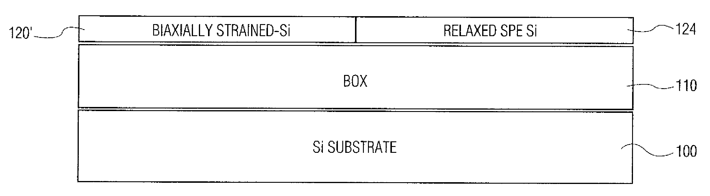
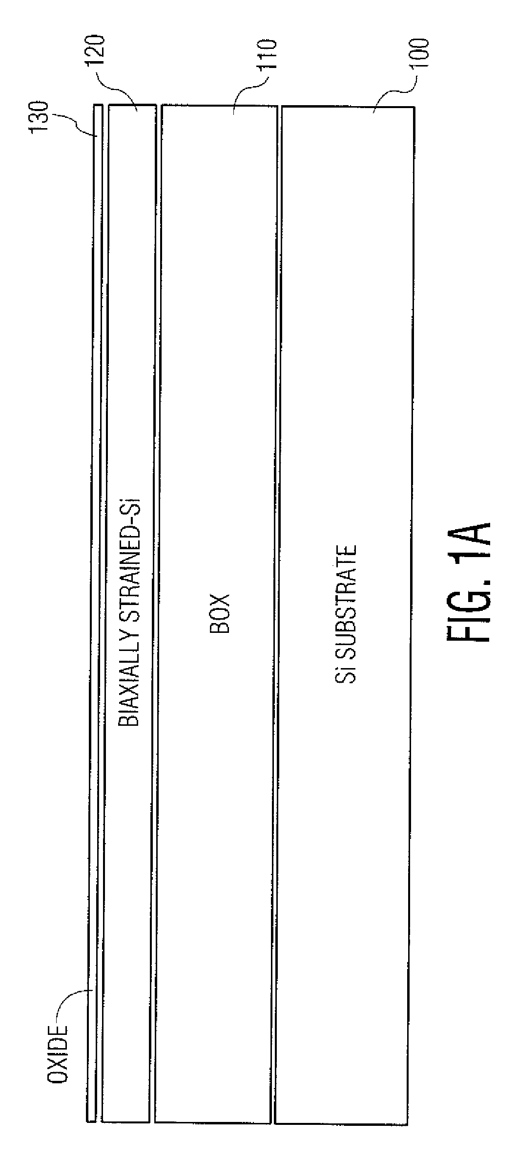
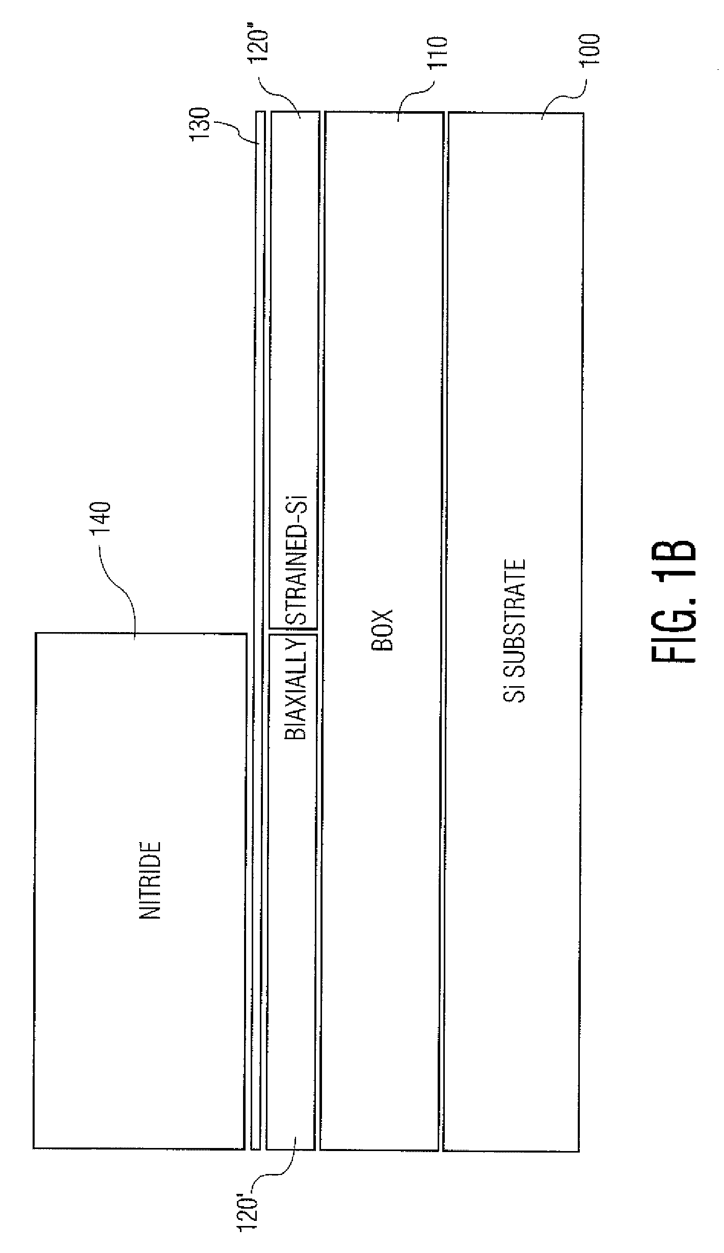
[0018]In a first embodiment, the invention comprises a method of forming a localized region of relaxed Si within a biaxial tensile strained Si layer (120) comprising a strained silicon directly on insulator (SSDOI) semiconductor substrate. The method steps for the first embodiment are dep...


PUM


Abstract

A method of forming a localized region of relaxed Si in a layer of strained Si arranged within a strained silicon directly on insulator (SSDOI) semiconductor substrate is provided by the invention. The strained Si layer is formed on a buried oxide (BOX) layer disposed on a Si substrate base. The method includes depositing a nitride hard mask pattern above a region of the strained Si layer in which enhanced electron mobility is desired, leaving an unmasked region within the strained Si layer, and carrying out various other processing steps to modify and relax the unmasked portion of the strained region. The method includes growing an EPI SiGe region upon the unmasked region using pre-amorphization implantation, and forming a buried amorphous SiGe region in a portion of the EPI SiGe region, and an amorphous Si region, below the amorphous SiGe region. Then, using SPE regrowth, modifying the amorphous SiGe and amorphous Si regions to realize an SPE SiGe region and relaxed SPE Si layer. The SiGe region and the SPE SiGe region are etched, leaving the relaxed SPE Si region above the buried oxide layer. The nitride pattern is stripped.

Description

[0001]The present invention relates broadly to strained silicon (Si) directly on insulator (SSDOI), and more directly to a method of forming biaxial strained silicon on insulator semiconductor substrate to include localized regions of relaxed Si.BACKGROUND OF THE INVENTION[0002]Biaxial tensile strained silicon (Si) directly on insulator (SSDOI) is a layer of silicon, typically disposed directly on dielectric layer formed on a semiconductor substrate, in which the silicon atoms are stretched beyond their normal interatomic distance. One way of straining silicon is to grow a layer of Si over a substrate of silicon germanium (SiGe). As the atoms in the Si layer align with the atoms in the SiGe layer, wherein the interatomic distances longer, atomic “links” become stretched, or strained (i.e., strained silicon). An increased distance between stretched or strained atoms reduces the atomic forces that interfere with the movement of electrons through transistors formed in the SSDOI, i.e., ...

Claims


Application Information

Patent Timeline
Patent Type & Authority Patents(United States)
IPC IPC(8): H01L21/36H01L21/20
CPCH01L21/02532H01L21/02664H01L21/26506H01L21/84H01L29/1054
Inventor LIU, YAOCHENGSADANA, DEVENDRA KUMARRIM, KERN
Owner IBM CORP
Why Eureka
Try Eureka