Organic electroluminescent device

a technology of electroluminescent devices and organic materials, which is applied in the direction of luminescnet screens, discharge tubes, natural mineral layered products, etc., can solve the problems of increasing drive voltage and power consumption, triphenylamine derivatives, and becoming very unstable upon accepting electrons, etc., to achieve low drive voltage and long life

Inactive Publication Date: 2006-02-09
SANYO ELECTRIC CO LTD
View PDF2 Cites 68 Cited by
  • Summary
  • Abstract
  • Description
  • Claims
  • Application Information

AI Technical Summary

Benefits of technology

[0011] An object of the present invention is to provide an organic electroluminescent device having a low drive voltage and long lifetime.

Problems solved by technology

Therefore, using Alq3 as an electron transporting layer increases drive voltage and power consumption in an attempt to inject sufficient electrons to the light emitting layer.
A triphenylamine derivative, typically used as the material of a hole transporting layer, becomes very unstable upon accepting electrons, and deteriorates.
This results in a shortened luminescent lifetime of the organic EL device.

Method used


Image

  • Organic electroluminescent device
  • Organic electroluminescent device
  • Organic electroluminescent device

Examples


first embodiment

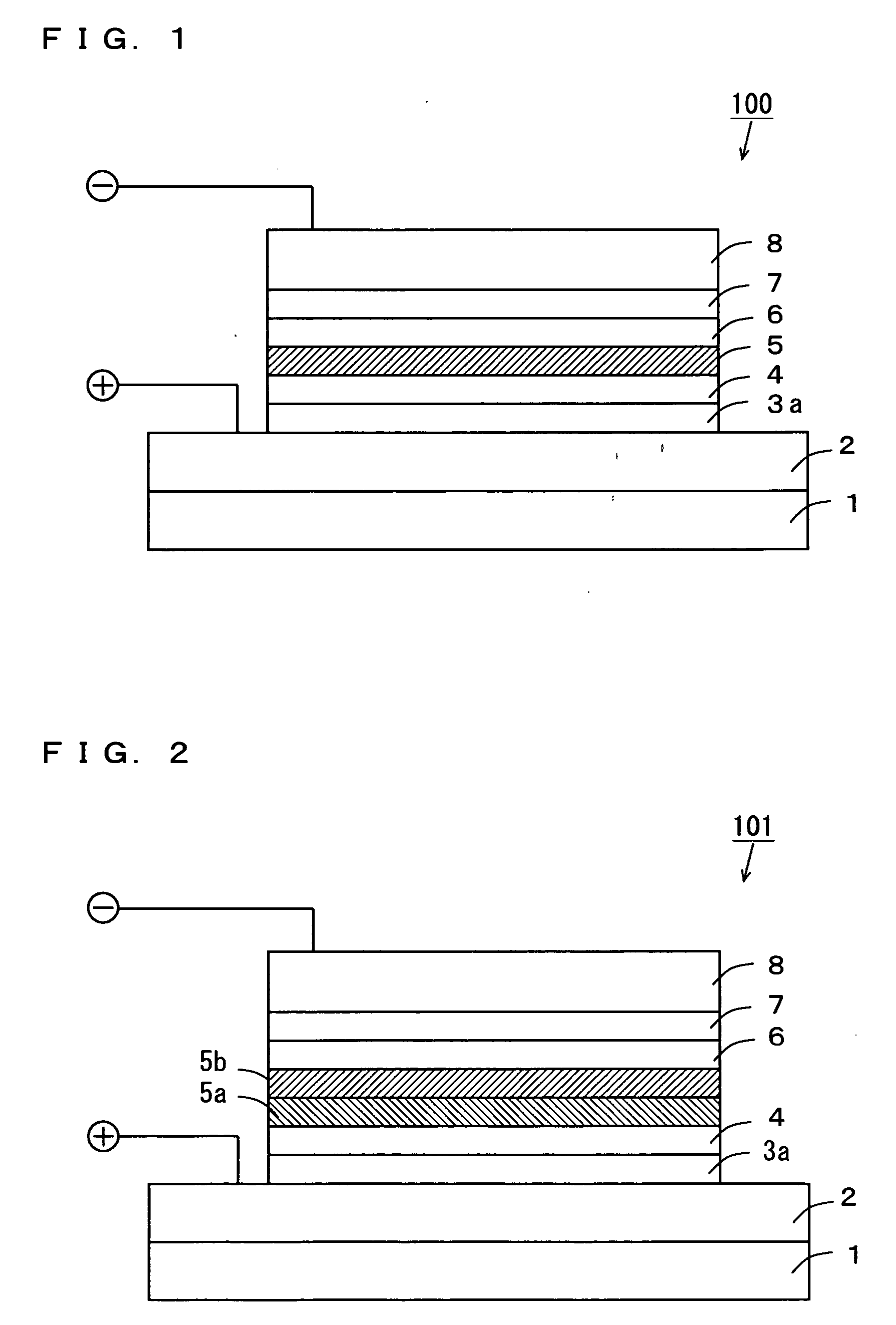
[0055]FIG. 1 is a schematic cross section showing an organic EL device according to a first embodiment of the present invention.

[0056] In fabricating the organic EL device 100 shown in FIG. 1, a hole injecting electrode 2 made of a transparent conductive film such as indium-tin oxide (ITO), for example, is formed first on a substrate 1. Then, on the hole injecting electrode 2, a hole injecting layer 3a, hole transporting layer 4, light emitting layer 5, electron restricting layer 6, and electron transporting layer 7 are formed in sequence. Further, on the electron transporting layer 7, an electron injecting electrode 8 made of aluminum or the like is formed.

[0057] The substrate 1 is a transparent substrate made of glass, plastic or the like.

[0058] The hole injecting layer 3a is made of CFx (carbon fluoride) produced by plasma CVD (plasma chemical vapor deposition) method, for example. The hole injecting layer 3a preferably has a thickness not less than 0.5 nm and not more than 5 ...

second embodiment

[0088]FIG. 2 is a schematic cross section showing an organic EL device according to a second embodiment of the present invention. The organic EL device 101 of the second embodiment has a structure similar to that of the organic EL device 100 of the first embodiment, except including an orange light emitting layer 5a capable of emitting orange light and a blue light emitting layer 5b capable of emitting blue light, instead of the light emitting layer 5 in the organic EL device 100 of FIG. 1.

[0089] The orange light emitting layer 5a includes, for example, NPB as a host material, tBuDPN as an auxiliary dopant, and DBzR as a luminescent dopant. In this case, the luminescent dopant emits light, and the auxiliary dopant plays the role of assisting in the emission of the luminescent dopant by encouraging transfer of energy from the host material to the luminescent dopant. This allows the orange light emitting layer 5a to produce an orange emission having a peak wavelength of greater than ...

third embodiment

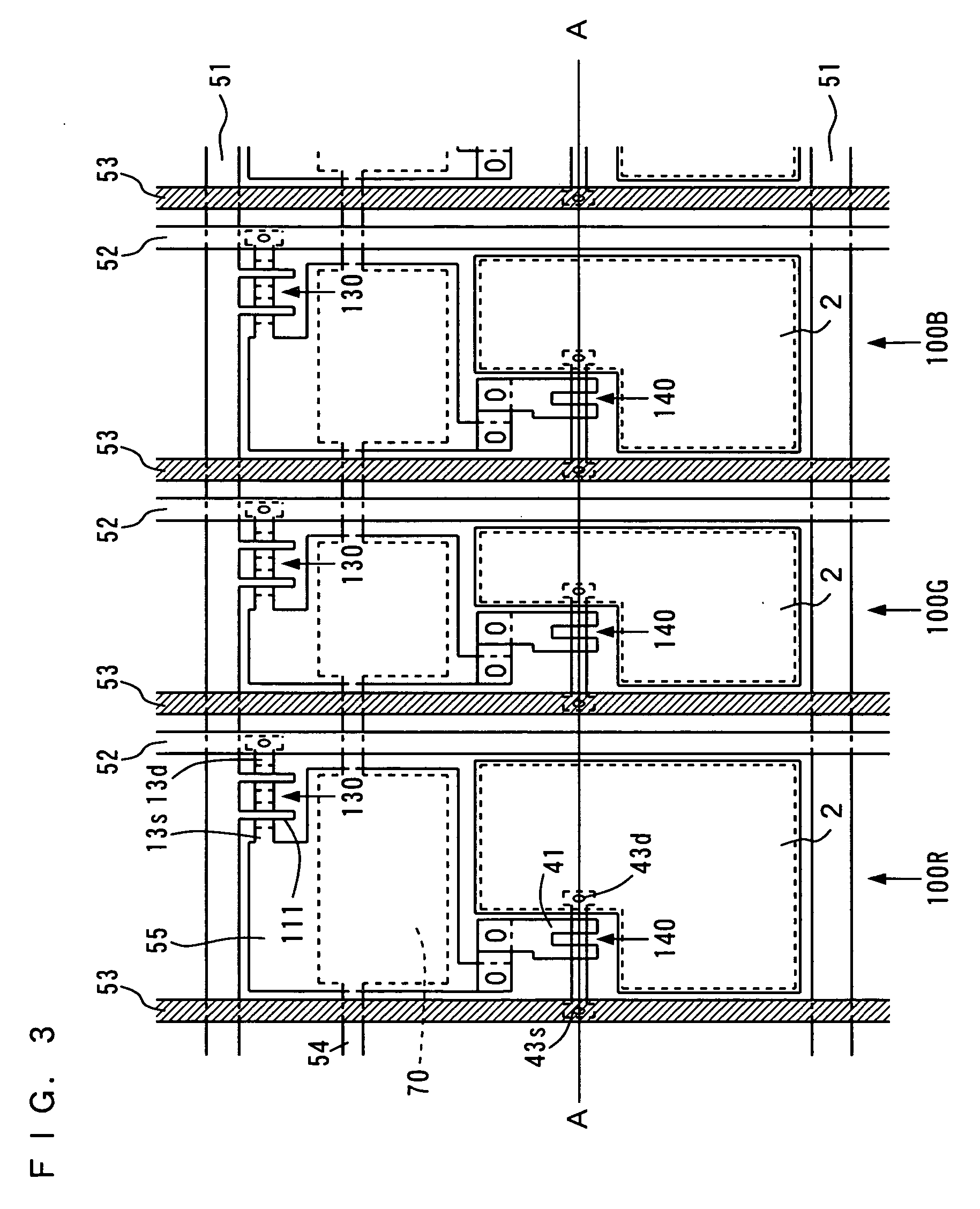
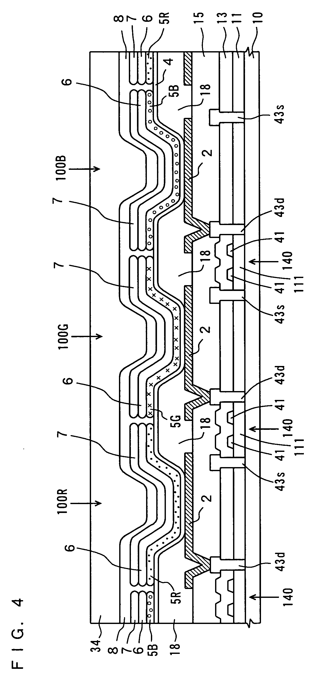
[0105]FIG. 3 is a schematic plan view showing an example of an organic EL display apparatus using organic EL devices, and FIG. 4 is a cross section of the organic EL display apparatus of FIG. 3 along the line A-A.

[0106] In the organic EL display apparatus of FIG. 3 and FIG. 4, an organic EL device 100R that emits in red, an organic EL device 100G that emits in green, and an organic EL device 100B that emits in blue are arranged in the matrix form.

[0107] Each of the organic EL devices 100R, 100G, 100B has a similar structure to that of the organic EL device 100 in FIG. 1. Each of the organic EL devices 100R, 100G, 100B comprises a red light emitting layer 5R that emits in red, a green light emitting layer 5G that emits in green, and a blue light emitting layer 5B that emits in blue, respectively, as a light emitting layer 5. The materials described in the first embodiment may be used for the light emitting layers 5R, 5G, 5B, respectively.

[0108] The organic EL display apparatus acc...


PUM

PropertyMeasurementUnit
peak wavelengthsaaaaaaaaaa
thicknessaaaaaaaaaa
thicknessaaaaaaaaaa

Abstract

An organic EL device has a structure that includes a hole injecting electrode, hole injecting layer, hole transporting layer, light emitting layer, electron restricting layer, electron transporting layer, and electron injecting electrode, in sequence, on a substrate. For the electron restricting layer, a material having an electron mobility lower than that of the electron transporting layer or a material having a low LUMO (lowest unoccupied molecular orbital) energy level is used.

Description

BACKGROUND OF THE INVENTION [0001] 1. Field of the Invention [0002] The present invention relates to organic electroluminescent devices. [0003] 2. Description of the Background Art [0004] With the recent diversification of information equipment, there is a growing need for flat panel displays that require lower power consumption than commonly used CRTs (cathode ray tubes). As one of such flat panel displays, organic electroluminescent devices (hereinafter abbreviated to organic EL devices) having such features as high efficiency, thinness, lightweight, and low viewing angle dependency have attracted attention. [0005] An organic EL device has a structure that includes, in sequence, a hole transporting layer, light emitting layer, and electron transporting layer between hole injecting electrode and electron injecting electrode. [0006] In conventional organic EL devices, in general, tris(8-hydroxyquinolinato)aluminum (hereinafter abbreviated to Alq3), for example, has been widely used ...

Claims


Application Information

Patent Timeline
Patent Type & Authority Applications(United States)
IPC IPC(8): H05B33/12H01L51/00H01L51/50H05B33/14H05B33/22
CPCH01L51/0054H01L51/0055H01L51/0058H01L51/006H01L51/0061Y10T428/24942H01L51/0073H01L51/0081H01L51/0094H01L51/5016H01L51/5096H01L51/0071H10K85/623H10K85/622H10K85/636H10K85/626H10K85/633H10K85/657H10K85/6574H10K85/324H10K85/40H10K50/18H10K50/11H10K2101/10E02B13/00
Inventor KANNO, HIROSHIOKUMOTO, KENJIHAMADA, YUJIHASHIMOTO, HARUHISAIYORI, MASAHIRONISHIMURA, KAZUKI
Owner SANYO ELECTRIC CO LTD
Why Eureka
Try Eureka