Photodetector array with background current compensation means

a photodetector array and compensation means technology, applied in the field of image sensors, can solve the problems of reducing the aspect ratio of the panel and relatively narrow dynamic rang

Active Publication Date: 2009-04-28
SHANGHAI XUANYAN ELECTRONICS TECH INC
View PDF4 Cites 17 Cited by
  • Summary
  • Abstract
  • Description
  • Claims
  • Application Information

AI Technical Summary

Problems solved by technology

The capacitors may require additional areas and therefore adversely reduce the aspect ratio of the panel.
Furthermore, the charges generated by a background light source and an input signal are equally stored in the capacitor, adversely resulting in a relatively narrow dynamic range.

Method used


Image

  • Photodetector array with background current compensation means
  • Photodetector array with background current compensation means
  • Photodetector array with background current compensation means

Examples


Embodiment Construction

[0021]Reference will now be made in detail to the present embodiments of the invention, examples of which are illustrated in the accompanying drawings. Wherever possible, the same reference numbers will be used throughout the drawings to refer to the same or like parts.

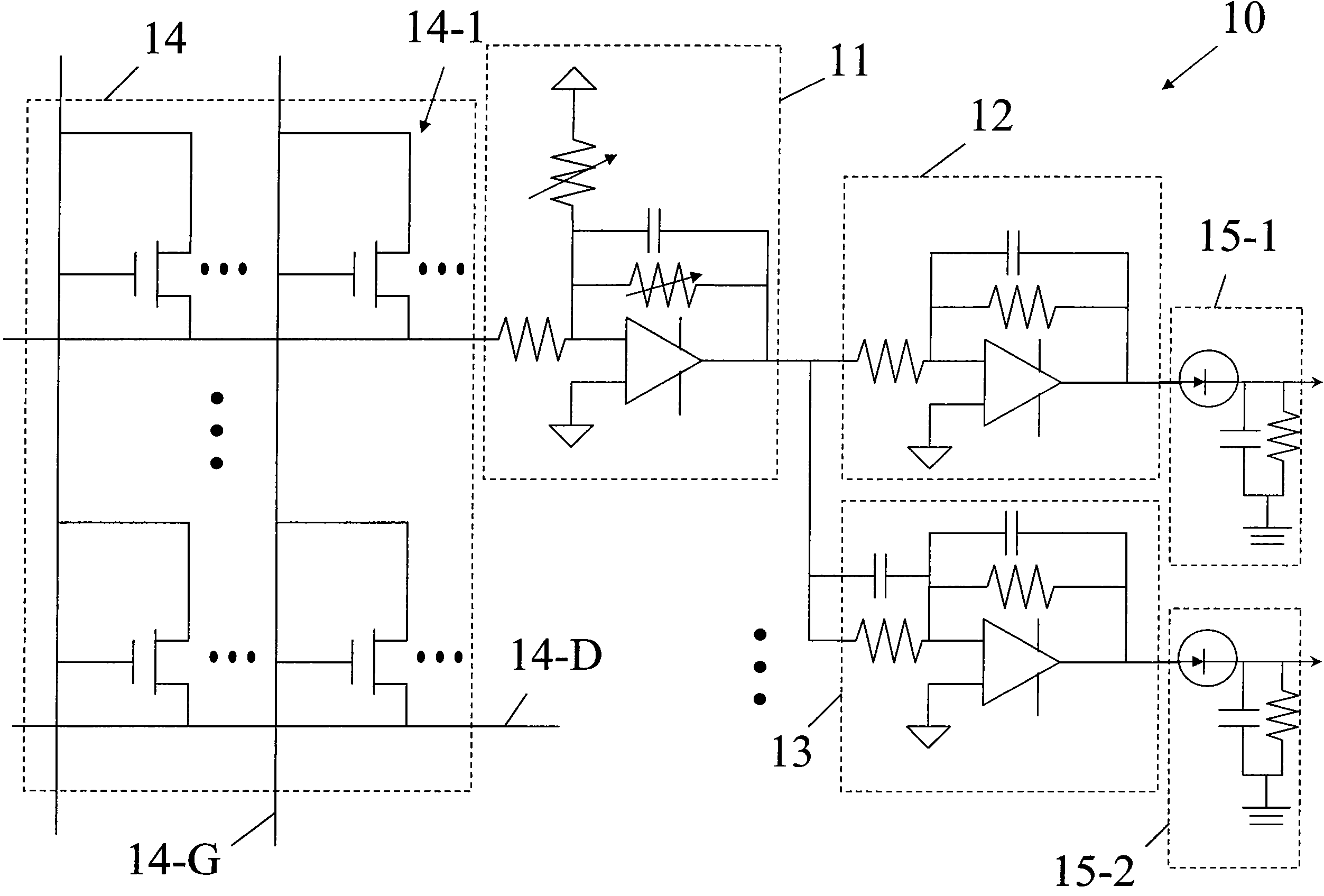
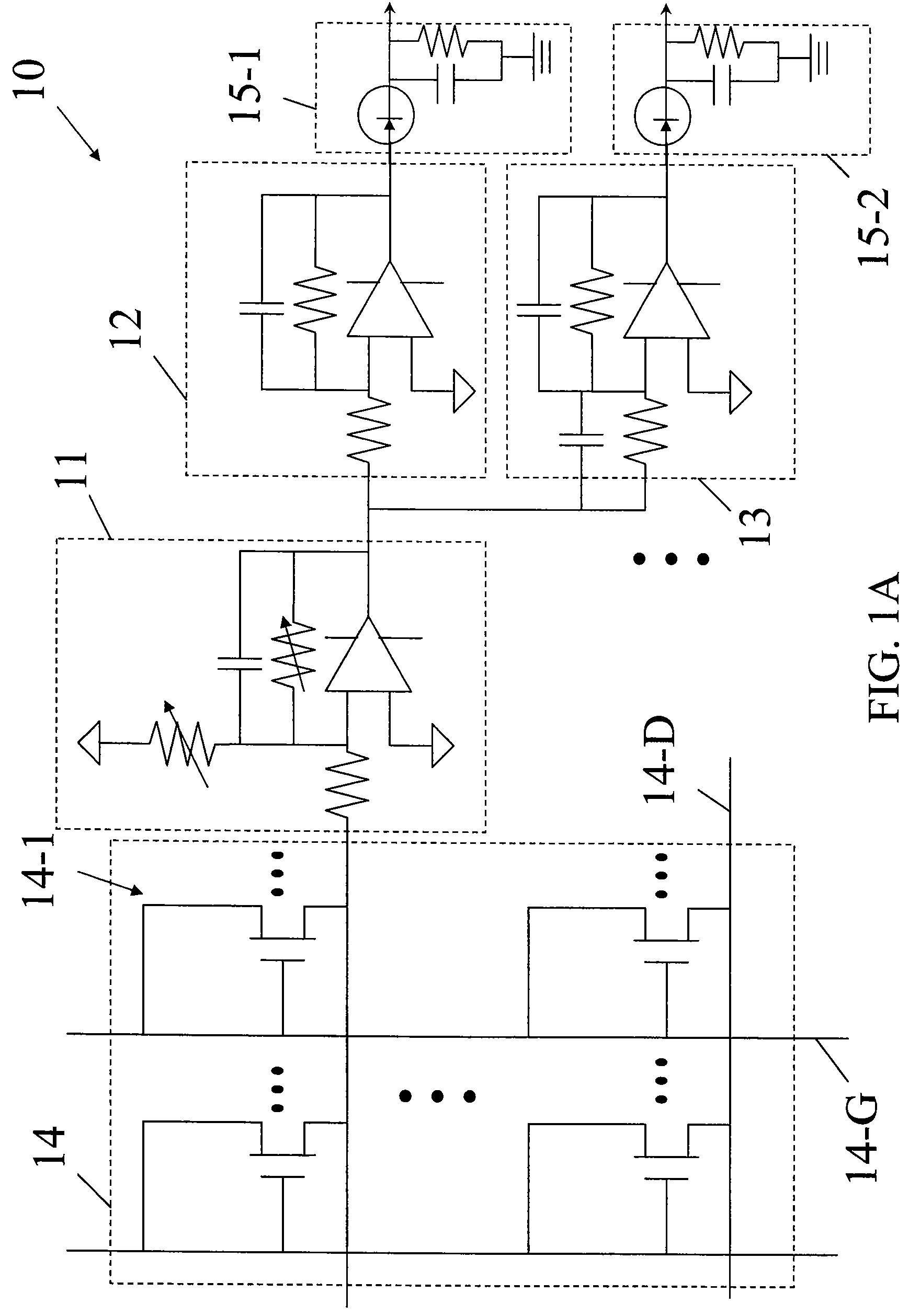
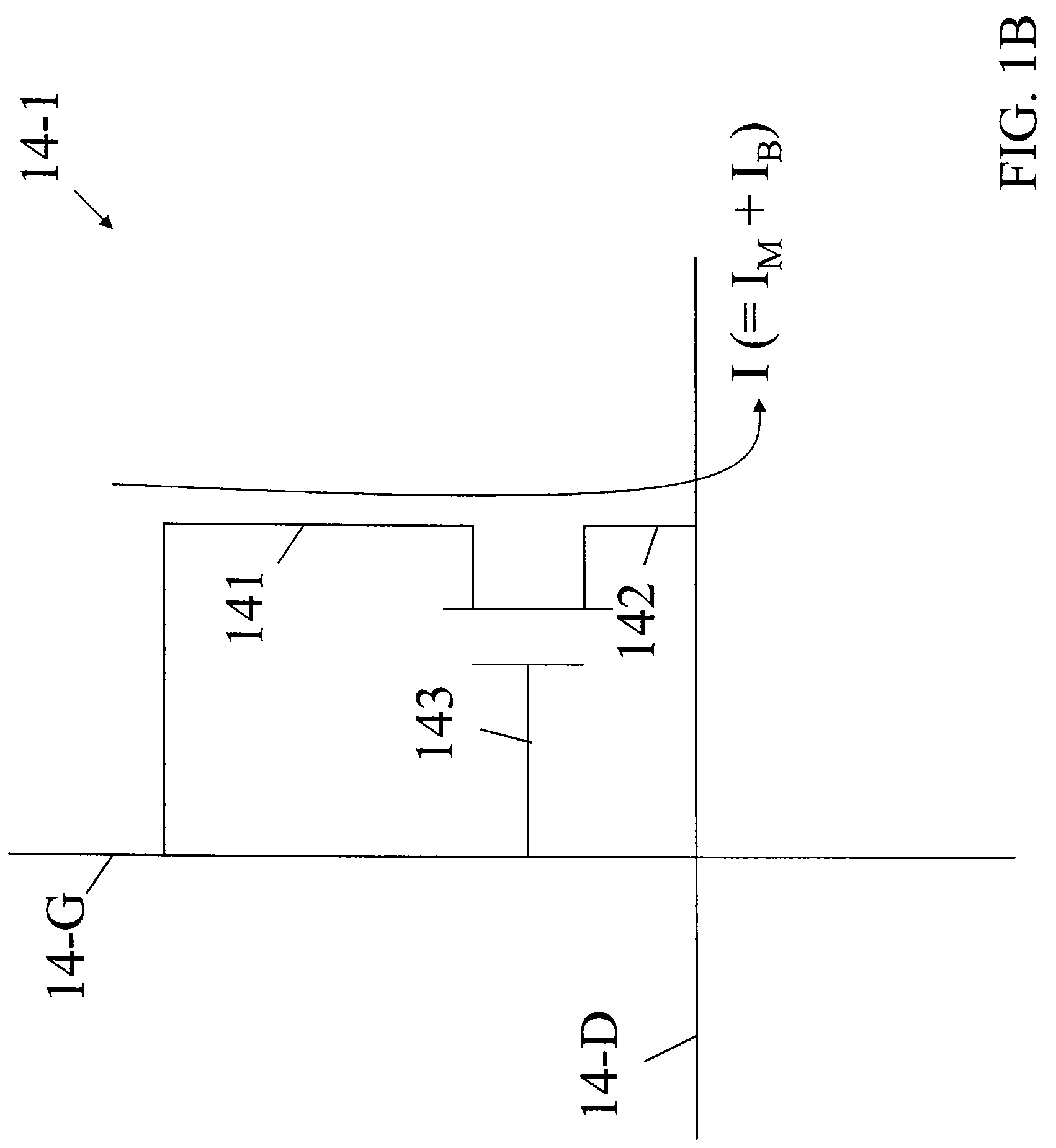
[0022]FIG. 1A is a schematic circuit diagram of a photo detector array 10 consistent with an example of the present invention. Referring to FIG. 1A, the photo detector array 10 includes a photosensitive transistor array 14, and a first amplifier module 11, a second amplifier module 12 and a third amplifier module 13 electrically connected to each row of the photosensitive transistor array 14. The photosensitive transistor array 14 includes a plurality of photosensitive transistors 14-1 formed in rows and columns. A representative photosensitive transistor 14-1 is disposed near an intersection of one of a plurality of gate lines 14-G and one of a plurality of data lines 14-D orthogonal to the gate lines 14-G. Each of t...


PUM


Abstract

A photo detector device includes a photosensitive transistor capable of detecting an optical signal including an image component and a background component and converting the optical signal into a current including an image current corresponding to the image component and a background current corresponding to the background component, a first amplifier module electrically connected to the photosensitive transistor capable of canceling the background current and amplifying the image current, and a second amplifier module electrically connected to the first amplifier module capable of detecting a direct-current (dc) portion of the image current.

Description

BACKGROUND OF THE INVENTION[0001]The present invention relates generally to an image sensor, and more particularly, to a photo detector device capable of detecting an image input from a stylus, pen, torch or a shadow.[0002]With the rapid development in the high-tech industry, pen tablets have been widely applicable to Personal Digital Assistants (PDAs), Personal Computers (PCs) and other electrical appliances used in our daily life. Generally, a pen tablet includes one of a resistor-type, electromagnetic inductance-type, capacitor-type and optoelectronic-type writing panel. As an example of the conventional optoelectronic-type pen tablet, an optical signal is converted into electrical charges, which in turn is stored in a capacitor of a detector array including capacitors, optoelectronic components and switch transistors before it is subsequently read. The capacitors may require additional areas and therefore adversely reduce the aspect ratio of the panel. Furthermore, the charges g...

Claims


Application Information

Patent Timeline
Patent Type & Authority Patents(United States)
IPC IPC(8): H01L27/00H03F3/08
CPCG06F3/0412H01L27/14681G06F3/042
Inventor FANN, SEN-SHYONG
Owner SHANGHAI XUANYAN ELECTRONICS TECH INC
Why Eureka
Try Eureka