
Dielectric device

a technology of dielectric devices and filters, applied in the direction of electrical equipment, multiple-port networks, waveguides, etc., can solve the problems of filter characteristics, failure to disclose a means, and fluctuation of pass band width, so as to improve filter characteristics such as the pass band width

Inactive Publication Date: 2009-05-19
TDK CORPARATION
View PDF29 Cites 0 Cited by
  • Summary
  • Abstract
  • Description
  • Claims
  • Application Information

AI Technical Summary

Benefits of technology

This configuration enables easy adjustment of filter characteristics, allowing the high-frequency attenuation pole to be shifted closer to the low-frequency side while maintaining stability of the low-frequency attenuation pole, thereby improving pass band width and frequency adjustment capabilities.

Problems solved by technology

Furthermore, a groove or recess may be formed in the dielectric substrate itself to intentionally upset the balance of electromagnetic coupling distribution for achieving electric field or magnetic field coupling.
When the dielectric device is mounted with the first and second terminals facing the circuit board, however, although most of an external conductor film connects with an earthing conductor on the circuit board through a solder or the like, electrical coupling between the earthing conductor and an intermediate conductor film, which is a part of the external conductor film, shifts an attenuation pole, resulting in fluctuation of pass band width and other filter characteristics.
However, this prior art document also fails to disclose a means to solve the above problems.

Method used


Image

  • Dielectric device
  • Dielectric device
  • Dielectric device

Examples


first embodiment

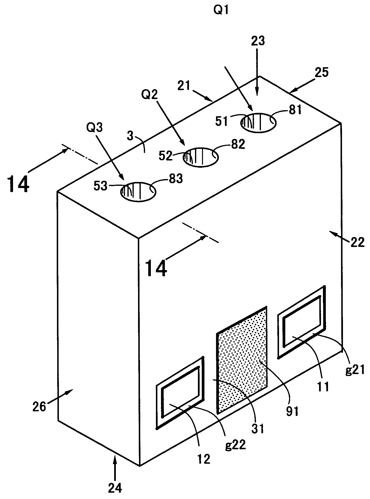
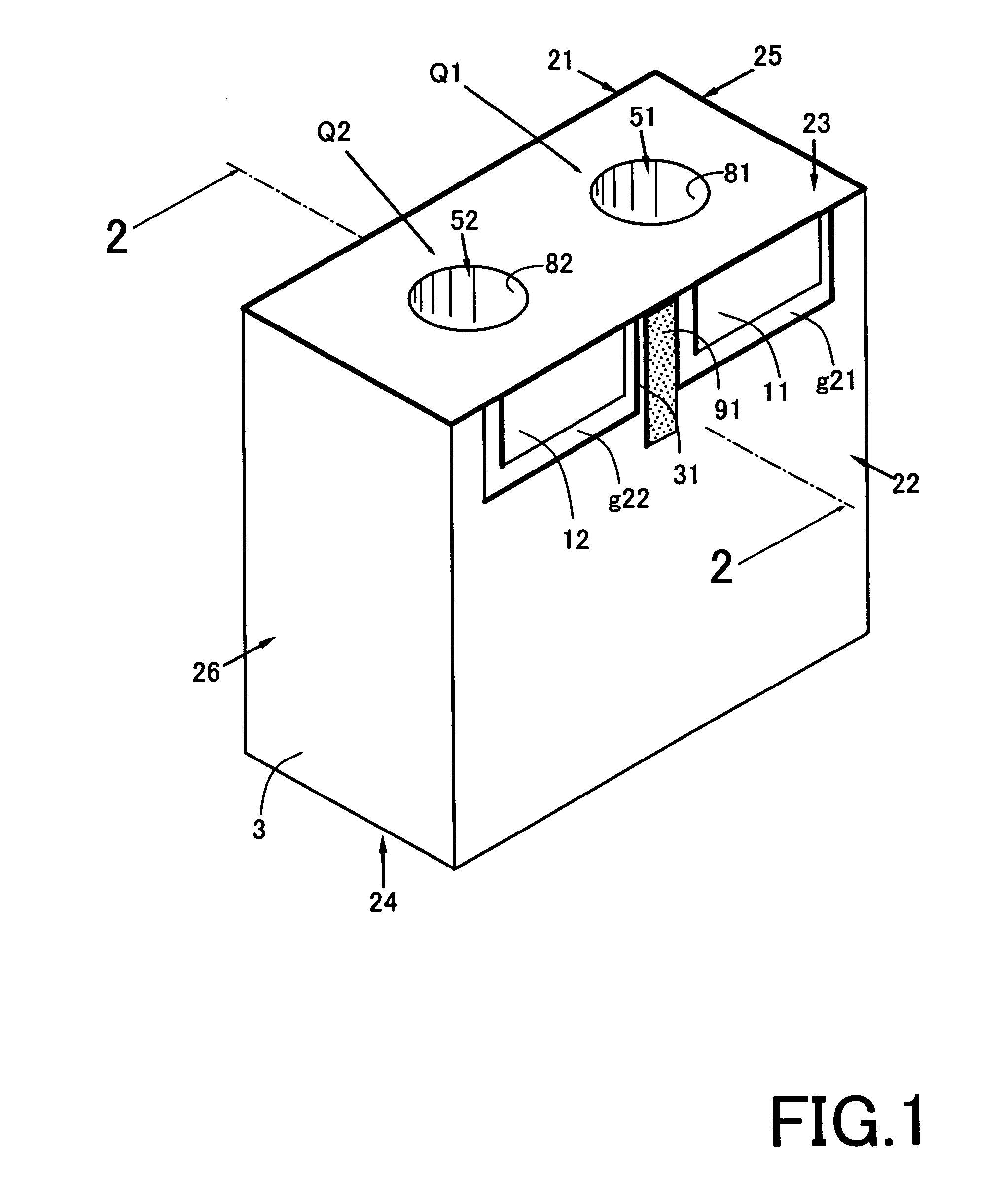
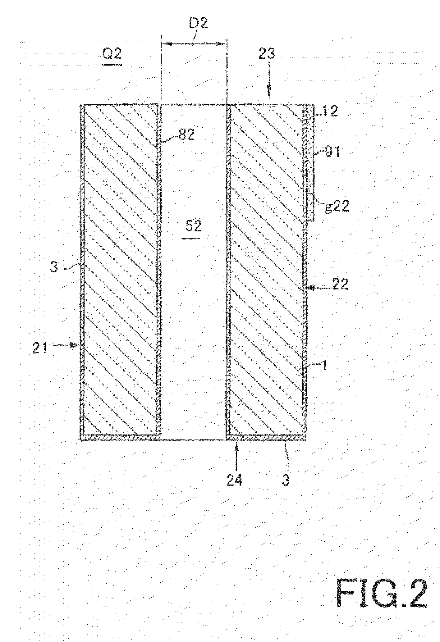
[0056]Referring to FIGS. 1 and 2, a dielectric device according to the present invention includes a dielectric substrate 1 and two resonator units Q1, Q2. The dielectric substrate 1 is formed from a well-known dielectric ceramic to have a generally hexahedral shape with first to sixth external surfaces 21 to 26. Typically, an external conductor film 3 may be formed by baking, plating or the like to contain copper, silver or the like as a main component.

[0057]The resonator unit Q1 includes a hole 51. The hole 51 opens on the third and fourth surfaces 23, 24 with an internal conductor 81 therein. The internal conductor 81 connects with the external conductor film 3 at one end opening on the fourth external surface 24. Alternatively, the internal conductor 81 may be formed by filling a part or the whole of the hole 51.

[0058]The resonator unit Q2, which has substantially the same configuration as the resonator unit Q1, includes a hole 52. Since the resonator unit Q2 has the same configu...

second embodiment

[0062]Referring to FIGS. 3 to 6, a dielectric device according to the present invention includes a dielectric substrate 1 and two resonator units Q1, Q2. The dielectric substrate 1 is formed from a well-known dielectric ceramic to have a generally hexahedral shape with first to sixth external surfaces 21 to 26. Typically, an external conductor film 3 may be formed by baking, plating or the like to contain copper, silver or the like as a main component.

[0063]The resonator unit Q1 includes first and second holes 41, 51. The first hole 41 is provided in the dielectric substrate 1 and extends from the first external surface 21 toward the opposite second external surface 22 with one end opening on the first external surface 21. The first hole 41 has a first internal conductor 61 therein. The first internal conductor 61 may be formed as an electrode film from the same material and by the same means as the external conductor film 3. Alternatively, the first internal conductor 61 may be for...

third embodiment

[0079]As understood from the foregoing description, the basic technical idea of the present invention is to separate the intermediate conductor film 31, which is a part of the external conductor film 3, from the earthing conductor 102. Accordingly, it may be embodied in a variety of ways as long as having the above function, for example, as shown in FIGS. 8 and 9 as a

[0080]Referring first to FIG. 8, the intermediate conductor film 31 is thinner than the first and second terminals 11, 12 to have a difference in surface level. With this configuration, although most of the external conductor film 3 connects with the earthing conductor 102 on the circuit board 101 through the solder or the like when the dielectric device 100 is mounted with the first and second terminals 11, 12 facing the circuit board 101, the difference in surface level between the intermediate conductor film 31 and the first and second terminals 11, 12 ensures separation of the intermediate conductor film 31 from the...


PUM


Abstract

A dielectric device includes a dielectric substrate, a plurality of resonator units, and first and second terminals. The dielectric substrate has an external conductor film thereon. Each of the resonator units has a hole and an internal conductor provided inside the hole and connecting with the external conductor film. The first terminal is provided on the dielectric substrate and electrically coupled with at least one of the resonator units. The second terminal is provided on the dielectric substrate and electrically coupled with at least another of the resonator units. An intermediate conductor film, which is a part of the external conductor film, is provided between the first and second terminals. The intermediate conductor film has an insulating film thereon.

Description

BACKGROUND OF THE INVENTION[0001]1. Field of the Invention[0002]The present invention relates to a dielectric device such as a dielectric filter or a duplexer and an electronic device using the same.[0003]2. Description of the Related Art[0004]Such dielectric devices are used in a high-frequency range such as sub-microwave band, microwave band, millimeter wave band, or sub-millimeter wave band. More specific examples of applications include satellite communication devices, mobile communication devices, wireless communication devices, high-frequency communication devices, or base stations for such communication devices.[0005]Conventionally, resonators and dielectric filters used in portable phones and the like have been constructed by combining a plurality of resonating units each formed by providing one through-hole in a dielectric substrate, wherein the resonator length is generally determined by dividing a quarter of a wavelength λ of a free space by the square root of a relative ...

Claims


Application Information

Patent Timeline
Patent Type & Authority Patents(United States)
IPC IPC(8): H01P1/20H01P3/06
CPCH01P1/2056H01P1/2136
Inventor TAKUBO, OSAMUTASHIRO, KOUJITERAO, KAZUYOSHI
Owner TDK CORPARATION
Learn More